Thinking about trying to match transistors. Got this cheap multi-function part tester which will show me Ube and hFE.
Which transistors should be matched, just the final output ones?
How do do you match? Do you
a) Match gain so both parallel NPN ones are the same, and both parallel PNP are the same
or
b) Match the NPN pair's average gain to be equal to the PNP pair's average gain? Don't you get grossly asymmetric amplification if there's a mismatch here?
Thanks!
Last edited:
Regarding my previous question, the answer is: Both, if you can. Although the PNP ones are unlikely to match their NPN counterparts, and also tend to scatter more. I think I found some good pairings tho among the 4 kits I have.
Is there any point in pairing any other transistors?
Also does anyone know the purpose of C3? Could I add a bypass ceramic cap to it? And I'm looking at replacing C4 and C6 with something better aswell...
Thanks
Is there any point in pairing any other transistors?
Also does anyone know the purpose of C3? Could I add a bypass ceramic cap to it? And I'm looking at replacing C4 and C6 with something better aswell...
Thanks
Thank you for your help and for sharing the sim file. Very appreciated.Tibia
Sorry for the late reply. I don't visit here often and I didn't realise that you only get notification for the first reply to your message. I didn't know a sub-thread had formed.
Firstly, please don't get me wrong. In no way was I throwing mud at LJM or the overall design, I have used part of the input stage in my own home amp. I'm trying to point out how the amp could so easily be improved and made more manufacturable by a few changes. It is made to be low cost and in fact has amazing distortion performance for such low cost. The biggest area in need of improvement is the bias circuitry. I think most people would agree that adjustment here is quite important. You will see in the attached MicroCap file that with default parameters throughout, the contribution to quiescent current from the driver transistor is considerably more than from the output devices. To be fair, I could not find spice files for the 2SA1186 or the 2SC2837 so have used replacements 2SA1837 and 2SC4793 as recommend here. It takes only a few very small tweaks to the R10/R19 bias chain values to restore something like normality. But there are still two problems there. 1-The bias current increases with temperature which can lead to thermal runaway. This can easily be fixed with a resistor of 10 to 20ohms in the collector of Q7 (stll take driver from Q7.C). 2-bias current imbalance between the two members of a pair (eg, Q2 and Q10). Unless you make deliberate changes, a simulation like this uses identical models for two instances of the same component. Translated to the real world that means it uses perfectly balanced pairs everywhere. I didn't realise myself just how important it is to match the members of a composite output set. Using the standard Vbe/Ic formula and a while with excel shows that a mismatch of only 5mV to 10mV can lead to one of the pair taking several times more current than the other, though the emitter resistor does partially mitigate this. I had heard the original manufacturer uses matched output pairs, but this could explain why some of the clones pop output devices so easily.
Some words on the attached MicroCap file. After I first used it I made changes and additions all over the place and haven't been very disciplined about keeping a backup chain. So I have recreated the file from the latest schematic I could find, which the poster here said was the same as on Calvins site. So be aware it is a brand new untouched implementation with no changes or configs anywhere. All of the transistor models that I've used should be incorporated into the file, so it should load and be ready to go. You can also reuse those models - search File Portability in the MicroCap help. I strongly suggest you put a pot between R10 and R19 and reduce there values to keep the total resistance of the chain roughly the same, and take the pot wiper to Q7 base.
Thanks Git for your in-depth analysis. So, thermal run-away is indeed a real possibility. Right now I am re-building abandoned L12-2 and have also ordered the most recent version. I hope to learn from this still unfinished project. I want to learn, not to make just a cheap "hi-fi" amplifier.1-The bias current increases with temperature which can lead to thermal runaway.
If you are worried about the mis-matching and/or blowing output transistor pairs, step-up the resistor values of the emitter resistors (0.22 Ohm)Thinking about trying to match transistors. Got this cheap multi-function part tester which will show me Ube and hFE.
Which transistors should be matched, just the final output ones?
How do do you match? Do you
a) Match gain so both parallel NPN ones are the same, and both parallel PNP are the same
or
b) Match the NPN pair's average gain to be equal to the PNP pair's average gain? Don't you get grossly asymmetric amplification if there's a mismatch here?
Thanks!
There are L12 amps with (tricky) emitter resistors as low as 0.1 Ohm.
Hello,
Starting from the file kindly shared by GIT (post #773) I have fired up Microcap 12 which now is free (FREE !!!)
My goal is to learn a few things and play with minor changes.
I made the minimal substitution needed to work with the default libraries of Microcap 12 plain vanilla :
2SA1015 -> KSA1015
2SC1815 -> KSC1815
2SC4793 and 2SA1837 models embedded in the circuit
2SD669->MJE344
2SB664-> MJE350
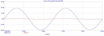
let's put aside for a second if those are the best substitution or not. I cannot get a decent bode plot (frequency response).
The transient analysis shows the amplification happens, but the response seems ... nonsense to me.
Any suggestion?
Thank
Tibia
Starting from the file kindly shared by GIT (post #773) I have fired up Microcap 12 which now is free (FREE !!!)
My goal is to learn a few things and play with minor changes.
I made the minimal substitution needed to work with the default libraries of Microcap 12 plain vanilla :
2SA1015 -> KSA1015
2SC1815 -> KSC1815
2SC4793 and 2SA1837 models embedded in the circuit
2SD669->MJE344
2SB664-> MJE350
let's put aside for a second if those are the best substitution or not. I cannot get a decent bode plot (frequency response).
The transient analysis shows the amplification happens, but the response seems ... nonsense to me.
Any suggestion?
Thank
Tibia
Attachments

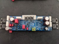
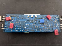
Almost finished my boards.
Changes from original:
Still waiting for C8 and then I'll have to clean the flux from the backside.
Changes from original:
- Quiescent current trimmers
- Since I had 4 boards, I matched each pair of Sanken output transistors to have their Ube and hFE as similar as possible
- Also matched the large output resistors
- Added a piece of aluminium to improve thermal coupling between Q7/Q5/Q9.
- Thickened exposed traces with additional tin
- C5 (33μF) will be replaced with off-board 2x10μF Wima film caps
- Feedback cap C8 (1000μF) will be replaced with 680μF Elna Silmic 2. Not soldered in yet.
- Replaced all caps ≤ 1μF with Wima film ones. Wasn't sure which caps affect the signal, so I just did them all. The small ones aren't super expensive.
- Replaced 100μF bypass caps with 330μF low-ESR ones. They have a slightly larger diameter, but I managed to make them fit.
- Also added 150nF film caps in parallel to the 330μF ones on the backside
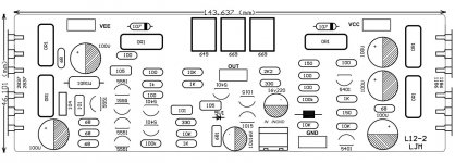
- C3 remained original 100μF part - I don't think it serves a bypass purpose. I don't know which purpose it serves at all.
Still waiting for C8 and then I'll have to clean the flux from the backside.
Attachments
Last edited:

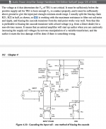
I don't think l12-2 needs to be modified.I have no understanding of these sorts of things, but I believe I've found what C3 does. Refer to the attached D. Self snippet and look at his C11.
Its circuit is not exactly the same as that of self.
Because everyone uses different components. Therefore, the circuit does not need to be the same. We just need to determine the final result.
L12-2 is the same as mx50se.Thanks Git for your in-depth analysis. So, thermal run-away is indeed a real possibility. Right now I am re-building abandoned L12-2 and have also ordered the most recent version. I hope to learn from this still unfinished project. I want to learn, not to make just a cheap "hi-fi" amplifier.
The thermal bias tube cannot be placed on the large radiator with the output power tube.
But need to be placed together with the drive transistor.
L12-2 will not change due to temperature. The quiescent current changes greatly.
of course. 10-20ma may change.
😛
you want to say that there is enough current through a 100kΩ resistor for a zener diode of 5.6 volts, or maybe, according to the datasheet, the current through the zener diode should flow at least 5 milliamps. The second point is that a cascade with an general base in the input differential stage is not needed, because input diffcascade converts to axial on the current mirror, the question is why?I don't think l12-2 needs to be modified.
I can only answer that if you power the amplifier from a high-voltage power source, for example, more than +/-50 volts, then it is only needed to unload the input differential stage, but in this case, instead of a 100 kOhm resistor, you need a stable current source, because. The diffcascade works with a common mode signal.
Oh. I know what you mean.you want to say that there is enough current through a 100kΩ resistor for a zener diode of 5.6 volts, or maybe, according to the datasheet, the current through the zener diode should flow at least 5 milliamps. The second point is that a cascade with an general base in the input differential stage is not needed, because input diffcascade converts to axial on the current mirror, the question is why?
I can only answer that if you power the amplifier from a high-voltage power source, for example, more than +/-50 volts, then it is only needed to unload the input differential stage, but in this case, instead of a 100 kOhm resistor, you need a stable current source, because. The diffcascade works with a common mode signal.
But there is actually no difference.
The current through the zener diode can be calculated. Which are currents between the input transistors VCE/ HFE. They are very weak.
The current through the diode is greater than this current.
Instead of 5 mA. How to get 5mA.
2SA1015 ICE= 2MA
i B= 2MA/ 200= 0.01MA (5.6V I>0.01MA )
VCE=50V R=100K I=0.5 MA
I don't think you need to put time on the 5V diode.
You can take measurements. These things do not cause any changes to the amplifier parameters.
Last edited:
Of course, that's why they are generally superfluous.))))These things do not cause any changes to the amplifier parameters.
But you put them so ridiculously - ok, let it be ....
I have tried and calculated this.Of course, that's why they are generally superfluous.))))
But you put them so ridiculously - ok, let it be ....
The current of this zener diode is not suitable to be larger. When the current is too large.
It generates noise. It is not recommended to change it.
But if it changes. There will be no obvious problems. Feel free to do this.
I often change these parameters. I've always changed. And then measured.
so I say that this block with a zener diode and transistors in the circuit is superfluous ...)))The current of this zener diode is not suitable to be larger. When the current is too large.
It generates noise. It is not recommended to change it.
But if it changes. There will be no obvious problems. Feel free to do this.
If this block is removed, the scheme will not be worse ...
In fact, the triode has one characteristic.so I say that this block with a zener diode and transistors in the circuit is superfluous ...)))
If this block is removed, the scheme will not be worse ...
It is an excellent triode. Their withstand voltage is very low.
Such as bc550c, mpsa18 and 2sa1015. Excellent transistors have these characteristics:
Minimal noise. Relatively high HFE and high performance. But their VCE is very low.
Generally less than dc45v.
In addition.
The input transistor operates at a lower voltage, such as 5V. Heat generation of the input transistor can be reduced.
It can reduce the noise generated by heat.
of course. If the operating voltage of the amplifier itself is relatively low. The coascode structure may not be used.
bc550c, mpsa18 - it's n-p-n pinoutSuch as bc550c, mpsa18 and 2sa1015.
2sa1015. - it's p-n-p pinout
we are talking about a circuit in which p-n-p conductivity at the input?
yes, that is what I said above, that an additional cascade in this circuit is needed if the power supply is high.Minimal noise. Relatively high HFE and high performance. But their VCE is very low.
Generally less than dc45v.
But because of this cascade, you incorrectly inserted the integrated common-mode correction R30C14 circuit, you need to put them at the high-resistance points of the cascade, where the anti-clip transistors are in the diode connection.
for this, it is necessary to organize the stabilization of the bases of the cascade with a common base correctly, for example, instead of R32, put a stable current source.The input transistor operates at a lower voltage, such as 5V. Heat generation of the input transistor can be reduced.
It can reduce the noise generated by heat.
I'm just giving an example. Bc550c or bc560c are similar.bc550c, mpsa18 - it's n-p-n pinout
2sa1015. - it's p-n-p pinout
we are talking about a circuit in which p-n-p conductivity at the input?
yes, that is what I said above, that an additional cascade in this circuit is needed if the power supply is high.
But because of this cascade, you incorrectly inserted the integrated common-mode correction R30C14 circuit, you need to put them at the high-resistance points of the cascade, where the anti-clip transistors are in the diode connection.
for this, it is necessary to organize the stabilization of the bases of the cascade with a common base correctly, for example, instead of R32, put a stable current source.
Second. You may have misunderstood me. In fact, l12-2 does not have C30 R14.
Resistance and capacitance are only used as components in the experimental circuit. And does not appear in the sales version.
Attachments
Ok , understood.I'm just giving an example. Bc550c or bc560c are similar.
this is good.Second. You may have misunderstood me. In fact, l12-2 does not have C30 R14.
Resistance and capacitance are only used as components in the experimental circuit. And does not appear in the sales version.
- Home
- Amplifiers
- Solid State
- L12-2 CFP Output amp 120W*2 8R