The 0R bypassing at output is for builders to try other bigger size capacitors.After some months, finally got around to finishing my kit.
Was fairly simple and enjoyable, start to finish maybe 3 hours, fairly straightforward and well marked (really, all those baggies precisely cut, well marked, etc..might have taken as much as it took to put the kit together, very nice (but your apartment must be littered with small baggies.. )
Tested all values on test points, everything fine from the get-go , but then i checked output and lo and behold 10V dc on the output.
Quick glance at the schematic shows two 0R resistors bypassing the DC blocking cap at the output, thus having DC again. Not sure exactly what their purpose is and why they're showed to be installed in the guide (or what to do with the ones marked SOT, or the how to select the phase resistor for the i2s shift register glue logic but i just put 0R to go to input A1 (first two squares)). Anywho no bigge issue solved in a second and on we go to listening.
I have to say sounds excellent. I really love this DAC, and at this price can recommend to anyone, abraxalito is doing the DIY community a big favour, especially the frugal audiophile. Another pro to some is no need for bipolar supplies. Plug in a single 20 and off you go.
That being said i have some other suggestions/questions...
1. only one GND on I2S input. I suppose done for space concerns/to keep the 4 pin connector. But really would have liked to see a 2x3, so each i2s line has it own separate current return path, in a twisted pair.
2.This one is more of a question, but not sure why some connectors are 90 degrees, and one is 0 degrees (straight up). Honestly i just straightened the 90 degrees one and now they all point up, not an issue just made me wonder if it has a purpose and i'll only realise i messed straightening them up later.
3. Not gonna lie, pretty big squeal on turn off...
4. I cheated a bit when i said it sounds great. It sounds great at really low volume (on headphones), in reality it begins to clip hard at around 0.1v (so says the DMM). At 0.15v its already making just fart noises, like someone recording a rock performance in the first row from their phone. Now since nobody else mentioned this i am assuming i just messed up somewhere. I thought maybe its the JLsounds board, but works great in any other dac. In the configuration sheet, i just used the standard I2S protocol (as for example an ES90xx dac). So i dont know, what the deal with that is, but yeah, im still feeling positive about this dac.
You could build a really neat little low-cost unit with this probably. Like those people on aliexpress, slap on a PCM 2706, in some generic case etc. JLCPCB is doing offers for pretty cheap smd assembly, and almost everything on the board is smd. Im just thinking out loud here, but this is a really neat little chip and abraxalito has been in the NOS tda1387 waters for a while. I guess hard part is getting the missus onboard with mass producing the inductors
P.S..merry ch
I believe the dac is designed to feed a pre or amp . The o.1v distortion is measured with what load?
Tested all values on test points, everything fine from the get-go , but then i checked output and lo and behold 10V dc on the output.
Quick glance at the schematic shows two 0R resistors bypassing the DC blocking cap at the output, thus having DC again. Not sure exactly what their purpose is and why they're showed to be installed in the guide (or what to do with the ones marked SOT, or the how to select the phase resistor for the i2s shift register glue logic but i just put 0R to go to input A1 (first two squares)). Anywho no bigge issue solved in a second and on we go to listening.
Apologies for the 0R resistor error, we'll make a correction to the build guide. The non-inverting position for R68 is to the left (towards I2S input).
The connectors are supposed to be all upright ones, so perhaps we made a mistake and sent you some 90o ones, apologies.That being said i have some other suggestions/questions...
1. only one GND on I2S input. I suppose done for space concerns/to keep the 4 pin connector. But really would have liked to see a 2x3, so each i2s line has it own separate current return path, in a twisted pair.
2.This one is more of a question, but not sure why some connectors are 90 degrees, and one is 0 degrees (straight up). Honestly i just straightened the 90 degrees one and now they all point up, not an issue just made me wonder if it has a purpose and i'll only realise i messed straightening them up later.
To me twisted pairs make sense when the frequency's high or the distance is long (or both), here in my estimation not worth the additional complication.
3. Not gonna lie, pretty big squeal on turn off...
Yes that's a downside of having only a single rail PSU.
4. I cheated a bit when i said it sounds great. It sounds great at really low volume (on headphones), in reality it begins to clip hard at around 0.1v (so says the DMM). At 0.15v its already making just fart noises, like someone recording a rock performance in the first row from their phone. Now since nobody else mentioned this i am assuming i just messed up somewhere. I thought maybe its the JLsounds board, but works great in any other dac. In the configuration sheet, i just used the standard I2S protocol (as for example an ES90xx dac). So i dont know, what the deal with that is, but yeah, im still feeling positive about this dac.
I took a look at the document and I see in the first group two settings for I2S that might be appropriate ('all DACs' and 'TDA1541'). The ES90XX setting is different. Without waveforms being shown I couldn't give confident guidance about which to choose.
The clip level is 2VRMS btw and no digital clipping happens even with inter-sample overs as there's headroom built in.
You could build a really neat little low-cost unit with this probably. Like those people on aliexpress, slap on a PCM 2706, in some generic case etc. JLCPCB is doing offers for pretty cheap smd assembly, and almost everything on the board is smd. Im just thinking out loud here, but this is a really neat little chip and abraxalito has been in the NOS tda1387 waters for a while. I guess hard part is getting the missus onboard with mass producing the inductors
The design can use the Mouser (Fastron or Bourns) 22mH, there are additional holes within the inductor silkscreen for them.
Thanks for the feedback, appreciated.
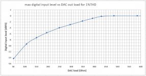
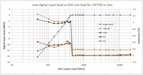
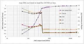
This DAC can drive loads above 500 Ohm without clipping, when fully driven (digital input level of 0dBFS). What is the impedance of your headphones?4. I cheated a bit when i said it sounds great. It sounds great at really low volume (on headphones), in reality it begins to clip hard at around 0.1v (so says the DMM). At 0.15v its already making just fart noises, like someone recording a rock performance in the first row from their phone.
Edit: Attached plots are for a 1kHz test signal
Please see last attachment and my post below:Now since nobody else mentioned this i am assuming i just messed up somewhere. I thought maybe its the JLsounds board, but works great in any other dac. In the configuration sheet, i just used the standard I2S protocol (as for example an ES90xx dac).
https://www.diyaudio.com/community/...ts-with-pre-built-filters.354799/post-6579227
George
Attachments
Last edited:
You're right should have specified. Some 32 ohm (nominal) headphones. Worked fine with any other DAC or thing i plugged them in so i didn't think about it much.The 0R bypassing at output is for builders to try other bigger size capacitors.
I believe the dac is designed to feed a pre or amp . The o.1v distortion is measured with what load?
Yup, will try these other settings. You're right though, without a scope trace it is guesswork, but i appreciate it, in any case one of these should work (assuming it is just I2S error, probably it is).I took a look at the document and I see in the first group two settings for I2S that might be appropriate ('all DACs' and 'TDA1541'). The ES90XX setting is different. Without waveforms being shown I couldn't give confident guidance about which to choose.
The clip level is 2VRMS btw and no digital clipping happens even with inter-sample overs as there's headroom built in.
EDIT: hit post before i saw George's comment.
Thanks for the info George, B1 and B3 it is (makes sense that it would be this really). Graphs are a nice bonus 🙂
Ah makes sense that you only got 0.1V into such a low impedance load. The output stage is current limited, you can get about 6mA in the positive direction. Which is nearly 200mV into 32R. I estimate you'll need to keep the digital attenuation above 23dB to avoid clipping. So the DAC effectively becomes about 12bit.You're right should have specified. Some 32 ohm (nominal) headphones. Worked fine with any other DAC or thing i plugged them in so i didn't think about it much.
A honest description of the mess due to improper loading 🙂At 0.15v its already making just fart noises, like someone recording a rock performance in the first row from their phone.
George
Attachments
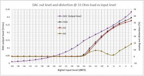
Yeah, makes sense then. Will have to listen to it with something else 🙂Ah makes sense that you only got 0.1V into such a low impedance load. The output stage is current limited, you can get about 6mA in the positive direction. Which is nearly 200mV into 32R. I estimate you'll need to keep the digital attenuation above 23dB to avoid clipping. So the DAC effectively becomes about 12bit.
Thanks for the help abraxalito and George
I have built the PhiDeca DAC and think it sounds great. How does the Kubelik differ form the PhiDeca DAC?
Debra
Debra
Debra - the Kubelik is a more compact PCB without the plug-in filter. It has a 3rd order filter on-board and the architecture is similar to DecaDAC, just not quite as low noise. Kubelik doesn't quite manage the same level of bass 'punchiness' as Deca, otherwise they are quite similar sounding. Kubelik has 6 paralleled DAC chips as against 10 on Deca.
And, as of today according to your beloved half, what about the sound of Celibidache vs Phi DecaDac version II?
Today during some more testing, I noticed a strange behavior.
DAC audio output was 10dB lower and distortion went up x10.
Test points TP9 and TP10 measure 17.4V instead of 10V. All other T.P. DC voltages are OK.
It is only when I touch with the probe resistors R19 and R45 that everything returns to normal (and stays normal).
The scenario repeats after power cycling, no matter if the DAC is warm or cold.
I have done all soldering again but this hasn’t changed anything.
Abrax, any idea ?
George
Hi George - interesting observations. TP9/10 go up to 17.4V but all the other TPs are normal? I'd be interested in knowing the voltages on TP6/7? If those are definitely normal then the issue could be oscillation in the output stage (Sallen-Key) opamp, which would be something I've not seen since adding in R71. Probing R19/45 seems to be applying damping to the oscillator.
And, as of today according to your beloved half, what about the sound of Celibidache vs Phi DecaDac version II?
We just did a comparison, using this CD : https://www.amazon.com/Shostakovich...takovich+dance+album,digital-music,305&sr=1-1
We both agreed the rhythm of the Waltz (2nd track) flowed better on Celibidache, it was easier to follow the individual strands. The difference wasn't huge though. Celibidache gets out of the way of the music more than Deca MkII.
Richard.
What is the voltage specifications for the resistors and capacitors used in Kubelik?
I intend to use the remnant parts for other projects in future .
Regards and Happy New Year
What is the voltage specifications for the resistors and capacitors used in Kubelik?
I intend to use the remnant parts for other projects in future .
Regards and Happy New Year
Resistors don't normally have a voltage spec - they're 0.125W rated for 0805 and normally we use 1% tolerance.
The SMD caps are various voltages - NP0s are normally 50V, the X7R/X5Rs will be less (16V for 1uF. 22uF I think). TH caps have voltages marked on them.
Happy New Year to all.
The SMD caps are various voltages - NP0s are normally 50V, the X7R/X5Rs will be less (16V for 1uF. 22uF I think). TH caps have voltages marked on them.
Happy New Year to all.
Its not a concern, no. The offset reflects under 300uA of current imbalance. If you like you can reduce the offset by fitting appropriate resistors for R69 and R70 (marked as SOT on the build guide). R70 = 2k and R69 = 3k will reduce the offset to 100mV or less.
- Home
- Vendor's Bazaar
- Kubelik NOS DAC kits