By GK:
By Lumba:
The ideas you presented are really interesting and hopefully you can further give us more details about your theories but off course better do it in another thread as a sign of respect to the contributor of this unique amplifier (at least for me). Your ideas are most welcome so that we can enhance our knowledge and learn alot more.
But with all due respect, pls start another thread to discuss your theories with other theorists. And for everyone to understand your ideas, why not put it into working circuit? In physics, your theories will only be theories and will never become a law if there's no proof. I am personally interested with your excellent ideas but in order to give a real contribution to everyone even with the other experts. Pls dont just say the thing is right or this is wrong, your theory is just a theory without a working circuit.
From this thread you can see alot of experts who simulated the circuit up to the minute details and directly/indirectly tell the author that his work is not working that the THD is not that low. I'm not the author but there's a feeling of stinging irritation and insult from those comments. Pls prove your claims by building the circuit not just by simulations then tell us your actual measurements, then you can prove everyone that your theories are correct, everyone will learn and will not forget you for proven contribution. Again, I have nothing against simulations but maybe you can also put into question the programs used for simulation besides most programs need de-bugging and by next year (most certainly) a new update will be released???
By now we can say that this amp circuit is not just a theory because its proven working not just by simulation but by actual building and measurements (pls don't ask me if I have proof). If you have doubts about the claims don't just talk but prove it, who knows you might even come up with better working circuit switching or non-switching and many will be very glad if you can graciously offer to the community.
Rgds,
mannycc
If I can't convince anyone who believes that this circuit is non-switching of the most obvious and easilly pointed-out boo-boo then there is little point in going any further.
By Lumba:
Hi, if working as intended, this circuit could at most eliminate switching distortion but not crossover distortion. Switching distortion can be easily and reliably prevented by class AB biasing without the strongly nonlinear transfer characteristic of this arrangement.
The ideas you presented are really interesting and hopefully you can further give us more details about your theories but off course better do it in another thread as a sign of respect to the contributor of this unique amplifier (at least for me). Your ideas are most welcome so that we can enhance our knowledge and learn alot more.
But with all due respect, pls start another thread to discuss your theories with other theorists. And for everyone to understand your ideas, why not put it into working circuit? In physics, your theories will only be theories and will never become a law if there's no proof. I am personally interested with your excellent ideas but in order to give a real contribution to everyone even with the other experts. Pls dont just say the thing is right or this is wrong, your theory is just a theory without a working circuit.
From this thread you can see alot of experts who simulated the circuit up to the minute details and directly/indirectly tell the author that his work is not working that the THD is not that low. I'm not the author but there's a feeling of stinging irritation and insult from those comments. Pls prove your claims by building the circuit not just by simulations then tell us your actual measurements, then you can prove everyone that your theories are correct, everyone will learn and will not forget you for proven contribution. Again, I have nothing against simulations but maybe you can also put into question the programs used for simulation besides most programs need de-bugging and by next year (most certainly) a new update will be released???
By now we can say that this amp circuit is not just a theory because its proven working not just by simulation but by actual building and measurements (pls don't ask me if I have proof). If you have doubts about the claims don't just talk but prove it, who knows you might even come up with better working circuit switching or non-switching and many will be very glad if you can graciously offer to the community.
Rgds,
mannycc
G.Kleinschmidt said:
That is why I wrote (in a following post):
.....(assuming, for the sake of the argument, the bias generator performs as advertised without the capacitor).
If I can't convince anyone who believes that this circuit is non-switching of the most obvious and easilly pointed-out boo-boo then there is little point in going any further.
Some people here have even proclaimed that the bias voltage is not dynamic (fixed) while continuing to insist that this OPS is non-switching.= appropriate smilie.
Actually, Steve said there is no signal voltage over the capacitor:
http://www.diyaudio.com/forums/showthread.php?postid=1757888#post1757888
Third and fourth paragraph: The AC voltage between the emitters of the bias pair remains constant (well very close). I thought I had answered your last question. I may have done that in a thread started on another DIY site. There is not an AC voltage drop across that cap. If you look at either side of the cap, you will see an exact replica of the input signal throughout the entire cycle. If you look at both sides of the cap differentially, there is no signal.
post 1169.
C2 is the normal Miller comp cap.
Best sound if you can get the amp stable without it.
That appears to be why Steve has chosen to make it optional and very low in value if fitted.
Steve's adoption of VAS to LTP feedback virtually removes the need for the Miller comp cap and can result in both good sound and very low distortion around the two stages of the voltage amplifier.
Let me summarize the last couple of days and give my take on the bias string. I also think I can suggest a few easy experiments that anyone can try in order to see what I mean.
The base currents of Q8 and Q10 must be equal. Since it is highly unlikely that their betas match one or the other saturates until this is true. This is easily confirmed by trimming one of the 10mA bias currents until the saturation region switches sides. The transition is about 800-900mV and takes only about .75mA to go from top to bottom. At just the right current the offset is 0 and Q8 and Q9 share the voltage. In Andy’s circuit this happens when Q1 has 5-6 mA more current. Since the output darlington is unlikely to demand that much current on a DC or low frequency basis this switching will never occur here. It is also highly unlikely that this voltage would compensate the Vbe related crossover transition anyway. As I said yesterday this voltage appears in series with the input and can not help keep the output from switching, in fact as was pointed out explicitly the output stage delta Vbe's are held constant.
To put some numbers on the currents. The output darlington has no resistor across Q13 and Q16’s bases so at 25mA of bias there is only a few microamps of input current. Even at several amps of output current this current hardly gets into the mA region. At 10mA in the bias string this means the betas of Q8 and Q10 as well as the current sources would have to match +-10% at these operating points for any switching action to take place. It is possible but highly unlikely that both devices sit saturated at just the right voltage to light up the output stage at just the right current. Devices would have to be selected on absolute Vbe and Vsat basis to get things to line right up.
In any case each set of parts will do something a little different. With the devices in Andy’s file the saturation never switches at any bias setting. I see no reason that many real devices wouldn’t behave in a similar manner.
So one experiment is to add a trim on one or the other 10mA bias currents in addition to the output bias trim and see if anything interesting happens. I went back to Andy’s sim and trimmed the offset to 0, neither device is fully saturated, and the behavior still shows 3400 Ohms as the optimum point. This is about the same point as Barney Oliver showed in 1972. The collectors move on Q8 and Q10 but only on current demand to the output not at crossover.
I have no idea about the observed distortion null. If someone can observe it and then poke around there will be a physical reason for the behavior.
bear said:Glen, you have a high level of expertise, it would be beneficial to most readers here if you would illuminate your concerns regarding the cap and the issue of switching.
I'm not Glen, but I think we have the same position regarding the switching vs. non-switching issue. So I'll give this one a try. Please note that what follows is not intended as any sort of criticism of the circuit, but just a discussion of circuit operation. Also some will consider the explanation below to be verbose and belaboring the obvious. Sorry about that.
Let me begin with an anecdote. Back in my school daze, I was in a class where the instructor was talking about some logic circuits implemented as discrete transistors. Confused by the apparently arbitrary assumptions about the states of various transistors, I asked him, "But how do you know the transistor is in that state"?
He replied, "You don't necessarily. You have to make some assumptions, then apply Kirchoff's voltage and current laws. If you arrive at a contradiction, at least one of your assumptions must have been wrong. Then you'll have to try some different assumptions".
That's good advice. I'll follow it below. Specifically, I'll look at two assertions that have been put forth as being simultaneously true, namely:
A) that the voltage difference between the bases of the output transistors is constant, and:
B) that the circuit is non-switching
There are five voltage drops to be considered for the output devices. They are:
1) The voltage between the output device bases. This is the voltage at the NPN base minus the voltage at the PNP base. Call it Vbb.
2) The base-emitter voltage of the NPN (base voltage minus emitter voltage). Call it VbeN. VbeN is positive in the active region of the NPN.
3) The voltage across the NPN's emitter resistor (NPN emitter voltage minus output voltage). Call it VrN.
4) The voltage across the PNP's emitter resistor (output voltage minus PNP emitter voltage). Call it VrP.
5) The emitter-base voltage of the PNP (emitter voltage of PNP minus base voltage of PNP). Call it VebP. VebP is positive in the active region of the PNP.
Kirchoff's voltage law says the sum of the last four voltages must add up to the first. Taking them in order from the first to the fifth, we have:
Vbb = VbeN + VrN + VrP + VebP
Let's look at the quiescent state first. Assume that in this state, VbeN = VbeP = 0.6V. Let's also assume 25 mV across each emitter resistor, for a total voltage of 50 mV across the series combination. This gives a DC current of about 114 mA, which is a pretty typical value. The result is that the voltage difference between the bases (Vbb) must be 0.6 + 0.025 + 0.025 + 0.6 = 1.25 Volts.
By the assumption (A) above, the voltage difference Vbb between the bases of the output devices must be 1.25 Volts under all conditions. Let's now assume that the amp is sourcing about 5A peak. Specifically, assume the NPN is sourcing exactly 5A. A typical power transistor might have Vbe of somewhat more than 0.8V under this condition. Let's assume it's exactly 0.8V to get a round number. The voltage drop VrN across the NPN's emitter resistor will be 5A * 0.22 Ohms = 1.1 Volts under this condition. Adding these two together, VbeN + VrN = 0.8 + 1.1 = 1.9 Volts.
So now on the left side of the equation above for Vbb, we have Vbb = 1.25 Volts, and VbeN and VrN add up to 1.9 Volts. This means we need some negative numbers for either VrP or VebP or both for Kirchoff's voltage law to hold. Let's assume the PNP is in the active region. This means VebP > 0. Since VbeN and VrN already add up to a number that's greater than 1.25 Volts, adding a positive VebP to that will make the right side of the equation greater still. Thus, for Kirchoff's voltage law to hold under the assumption that the PNP is in the active region, VrP must be negative. However, that could only happen of the emitter of the PNP were sourcing current. That can't happen. Since the PNP can only sink current at its emitter, VrP must be positive or zero. But if VrP were positive, then the PNP would be sinking a non-zero current and VebP would be positive too. But then Kirchoff's voltage law would not hold. Therefore, the only valid value for VrP is zero. This in turn means that VebP must be negative, which means the base-emitter junction of the PNP is reverse biased. Ignoring charge storage effects, the conclusion is inescapable - the base-emitter junction of the PNP is reverse biased under this condition and the PNP is OFF.
Of course, if you reverse bias the base-emitter junction of a BJT, it won't turn off immediately. If you want to turn if off really fast, then for at least a brief period of time, the instantaneous base current must be in the opposite direction of the normal operating DC current. If you look at the schematic of the Krill, the arrangement with the drivers does not allow that to happen. So the output device that's turning OFF will do so relatively slowly. This can be easily seen in a simulator.
In short, if you assume that the voltage difference between the output device bases is constant under all conditions, application of Kirchoff's voltage law to the output stage under high-current conditions leads to the conclusion that the nominally inactive transistor must turn completely OFF. Using a similar line of reasoning, if one assumes that the nominally inactive transistor does not turn OFF, one is led to the conclusion that the voltage difference between the bases cannot be constant. I won't do that part as this post is already too long.
jkeny said:OK, I'll come clean - for the last week I've been in bed with bad sciatica - trying to keep the pain down with Valium, Codeine & Diffene. So when not dealing with the pain & feeling "comfortable numb", I'm bored out of my mind other than having you guys for company, that is
Take care of yourself and get well soon Mate!!

I know a couple of nice looking nurses that could motivate you to get moving - but they live in Nashville so you'll need to find some of your own.
A request to builders. Please trim the bias to 25mA and then measure the distortion without applying global feedback as at least one data point.
The circuit remains a nice trick to bias a triple follower and independently adjust the input follower current and output current.
The circuit remains a nice trick to bias a triple follower and independently adjust the input follower current and output current.
Good post Andy_C,
That's the sort of useful post where assumptions, hypotheses and conclusions are elucidated and a way forward can be plotted to test these! I guess we have to wait for some real tests to evaluate this hypothesis.
Scott, can you post the circuit you're referring to - I can't make sense of your component identifiers?
Thanks Thomas, how is your wife now - fine I hope! And the dog doing well also? I'm afraid good looking nurses would only frustrate me with a bad back you understand!
jkeny said:Good post Andy_C,
That's the sort of useful post where assumptions, hypotheses and conclusions are elucidated and a way forward can be plotted to test these! I guess we have to wait for some real tests to evaluate this hypothesis.
Scott, can you post the circuit you're referring to - I can't make sense of your component identifiers?
Thanks Thomas, how is your wife now - fine I hope! And the dog doing well also? I'm afraid good looking nurses would only frustrate me with a bad back you understand!
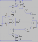
What a pain, I had hoped andy_c had preserved the original Q numbers. They are in his LTSpice post. Q8 and Q10 are the devices that operate at or near saturation Q8 and Q11 in the original schematic. My Q1 is Q9 the top current source and the other two devices are the outputs that are labeled X13 and Q14 in the original. I also misspoke. When you get the offset just to 0 I said Q8 and Q9 share the voltage that should have been (my) Q8 and Q10. The voltage being about .45V in the out of saturation direction for each.
BTW from the same quote "exact replica" of the input appearing on either side of the cap means there is no switching due to the saturation either.
"If you look at either side of the cap, you will see an exact replica of the input signal throughout the entire cycle. If you look at both sides of the cap differentially, there is no signal.:"
scott wurcer said:What a pain, I had hoped andy_c had preserved the original Q numbers. They are in his LTSpice post.
It would be nice to post a graphic. To create one from an LTspice sim, open up the sim, and with the schematic showing, choose Tools, copy bitmap to clipboard. Then paste it into your graphic viewer of choice and save as a PNG file (not JPG) from your graphics viewer (after cropping as necessary).
I'm not sure if the reference designators of the sim I posted will match yours, since it's possible that you did some editing that could have changed them.
Member
Joined 2009
Paid Member
troystg said:Post 809 has the BOM for all the parts.
Go to Mouser and Digi-key to see if you can afford it.
I was kind of hoping somebody had built this thing and could throw out an estimate. But after wading though so many posts I can hardly find any mention of anyone building one and listening to it. I hadn't realized that I'd wandered into a theoretical design discussion, it's too early to be choosing a design like this when it seems it's hardly moved off the drawing board ?

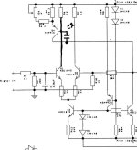
OK here's my schematic. And I just noticed that I misread the screen when the image was small. Q9 and Q10 are the pair of devices that are of concern so my little description is confusing, sorry. I was most concerned with the discussion about saturation and if this is why the sims don't match "reality".
I have also noticed another property of this circuit that really is different. The common mode level of the drive to the output stage is not driven as stiffly as when there is a follower directly connected to it. The base charge moving around can make it move and this then appears in series with the input. I don't see this doing anything here but with real devices who knows? I only mention it because it would not be the first thing I would measure.
This also would qualify as a fortuitous empirical artifact if in fact there was some cancellation.
Attachments
Bigun, the discussions are theoretical, but the design is not. Draw out a PCB design, or lay one out on General Purpose Veroboard, following Steve's schematic. Only the driver and output transistors are on the heatsink with the 2 temperature sensing diodes; all other parts are independent and may be placed conveniently as per schematic. From all reports thus far, you should be more than pleased with the sound of the amp.
One can see that the output devices do switch off, simply by probing Ie of the output devices in Andy's simulation. One could also differentially probe the output device's emitter resistor in real hardware to also see the effect.
I come to the conclusion that the odd transistors in the bias string are in a sense pass transistors in the following way:
Trusting the reports that the circuit works, take the input and output voltage to be zero. Then the collector of Q9, for example, is one Vbe drop up from zero, and the emitter is two Vbe drops above plus the output stage emitter resistor drop. There should be at least some Vce available to keep Q9 out or only partially into saturation. If the beta of Q9 is high, then Ic is nearly equal to Ie and therefore the device is a pass device from a current perspective. Q9 will also maintain a small Vce as long as the other base emitter junctions remain forward biased, and so it is also a pass device from a voltage perspective. The design looks like a triple EF with a diamond first stage as I see it.
Interesting circuit!
Pete B.
PB2 said:The design looks like a triple EF with a diamond first stage as I see it.
Interesting circuit!
Agree
jkeny said:Good post Andy_C,
That's the sort of useful post where assumptions, hypotheses and conclusions are elucidated and a way forward can be plotted to test these! I guess we have to wait for some real tests to evaluate this hypothesis.
Scott, can you post the circuit you're referring to - I can't make sense of your component identifiers?
Thanks Thomas, how is your wife now - fine I hope! And the dog doing well also? I'm afraid good looking nurses would only frustrate me with a bad back you understand!
The wife is well and spending money faster than ever! This is a mixed blessing - but what the heck - she deserves it. Manfred the Wonder Dachshund is back to chasing critters and generally getting into or creating mischief like his old self! God Bless the little rascal!
As to the nurses being a problem due to a bad back - well there are a number of suggestions I could make - but that is getting a little to far OT - and would most likely be me put into the sin bin.
Good discussion going today kids. As it has been noted before - simulators simply (sorta) simulate! GIGO + operator skill + limits of software and "device models" = Hmmmm could work, looks interesting, guess I'll need to build one and find out what's really going on! You can "simulate" flying an aircraft - or car - or whatever ----- BUT it is different than actually driving the car or flying the aircraft. Just because you are an "ace" fighter pilot in some flight sim does not mean that you can jump into some jet fighter and go blasting around the sky's. Most likely your "ace"😉 will wind up in a big crater just off the end of the runway!
BTW - Heads up - on Steve's last posted schematic (post #805) resistor R1 vanished into thin air. That is a glitch and R1 should be in the circuit. 220 R.
c2cthomas said:
BTW - Heads up - on Steve's last posted schematic (post #805) resistor R1 vanished into thin air. That is a glitch and R1 should be in the circuit. 220 R.
Thanks.
BTW, for a good looking burse I'm willing to fly again to the US …
I was in New York last month and it was to cold to my taste …🙂
jkeny,
I cannot estimate its dynamic behavior but it is quite indifferent to me because of the meager outcome, even working perfectly. An approach aiming to substantially reduce crossover distortion in class B would be much more sexy and challenging. (With some kind of error correction, however, due to its harmful character, paying great attention to signal integrity. This would be something for people like traderbam and Jan).
I cannot estimate its dynamic behavior but it is quite indifferent to me because of the meager outcome, even working perfectly. An approach aiming to substantially reduce crossover distortion in class B would be much more sexy and challenging. (With some kind of error correction, however, due to its harmful character, paying great attention to signal integrity. This would be something for people like traderbam and Jan).
- Status
- Not open for further replies.
- Home
- Amplifiers
- Solid State
- Krill - The little amp that might...