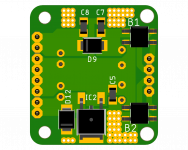
For dual 5V supplies , Prasi designed some nice little SMD boards with 500mA 78XX/79XX regs. All in one with bridge rectifiers. I wanted these to run a Muses volume and buffer boards direct from an AC winding.
Around 30 x 30mm
edit - maybe not these for the DAC IC, try LDOVR -
Dual Polarity
Around 30 x 30mm
edit - maybe not these for the DAC IC, try LDOVR -
Dual Polarity
Attachments

Last edited:
For dual 5V supplies , Prasi designed some nice little SMD boards with 500mA 78XX/79XX regs. All in one with bridge rectifiers. I wanted these to run a Muses volume and buffer boards direct from an AC winding.
I checked his site but didn't see these. Is there a schematic available? I'm also looking for single rail 5v psu's to power a usb bus and the smaller the better, so those 'cut in half' could be perfect.
Cool Jazz, the boards with extra LM reg section have been ordered, I'll let you have a couple when they arrive.
Very much appreciated! Are these from the schematic you posted or have there been changes?
No, Prasi designed the SMD 78XX/79XX for me, a custom request for a couple of little jobs where i needed a rectified SMD dual supply.
Yes the new adjustable boards are to the schematic posted.
Yes the new adjustable boards are to the schematic posted.
I checked his site but didn't see these. Is there a schematic available? I'm also looking for single rail 5v psu's to power a usb bus and the smaller the better, so those 'cut in half' could be perfect.
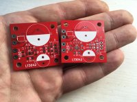
Cool jazz, i have you covered for the 5V USB supply, these little SMD LT3042 supply boards are spare, they are 35 x 35mm and 200mA output.
Schematic is to the datasheet. I'll send a couple with the other boards soon.
Attachments
Is there any benefit to having a dual channel design like in Juma's schematic from the first post in this thread? So separate circuits for left and right channel, coming from the same transformer secondary/rectifier block?
For the design in post #626, it isn't 100% clear to me what T1/2 and A1/2 are supposed to be.
Is T1 and T2 BCP56 and BCP53 and
A1/2 TIP41 and TIP43 ?
Correct.
I might try these for T1/T2, a bit higher HFE -
PZT2907A,115 Nexperia | Mouser United Kingdom
https://www.mouser.co.uk/ProductDetail/771-PZT2222A115/
For A1/A2 TIP31/32 will also do, any BJT with good gain. Toshiba 2sa1930/2sc5171 work well.
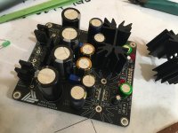
The new boards with regulators after the MX section are here. These now have option for TO-220 diodes or LT4320 SMD bridge PCB's. All resistors are SMD under PCB.
I think the procedure for these will be to build and trim the MX section first, then fit regs and finish adjustment. Retrospectively thinking, some test points for the MX section would be good.
I think the procedure for these will be to build and trim the MX section first, then fit regs and finish adjustment. Retrospectively thinking, some test points for the MX section would be good.
Attachments
Hi guys.
I've been trying to find these boards on various threads but to no avail so I hope you don't mind my asking here. Seems to be the place!
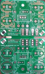
I got this board off a member here ( hello Rich!) and was wanting to read up a bit about it. I've sussed out the A1 and A2. Can I just stuff this board as per the silkscreen values?
I see most capmx on here have 10 to 30mF whereas this has a lot less.
What is the voltage drop from this board? Can someone link me to the process for setting the VR? What does this do exactly. I think I've read it adjusts the voltage drop and therefore the ripple reduction.? Or nothing like that at all.
Sorry for the beginner questions and thanks in advance.
James
I've been trying to find these boards on various threads but to no avail so I hope you don't mind my asking here. Seems to be the place!
I got this board off a member here ( hello Rich!) and was wanting to read up a bit about it. I've sussed out the A1 and A2. Can I just stuff this board as per the silkscreen values?
I see most capmx on here have 10 to 30mF whereas this has a lot less.
What is the voltage drop from this board? Can someone link me to the process for setting the VR? What does this do exactly. I think I've read it adjusts the voltage drop and therefore the ripple reduction.? Or nothing like that at all.
Sorry for the beginner questions and thanks in advance.
James
Attachments
Hi James, sorry should have given you more info, but your basically right.
This PCB is designed to go on the end of any rectified CRC supply - or between the caps for C->MX->C. You'll need a bit of filtering before these.
Stuff the board to the values - C2 1000uF is the multiplier cap with T1, so most important (can be higher uF), C1 sets the startup time with R4, the other two 1000uF are output caps so can be larger value.
T1 can be any BJT with pinout, TIP41/42, MJE ETC... higher hfe gain is better
The boards were designed by Prasi here, they appear near the end of the thread, - LT4320 based active rectifier
Last edited:
Thanks Rich
No worries...I did ask for this PCB off you and so you would be forgiven for thinking I know what to do with it!. I've been reading through Prasi's thread but didn't see this exact board although plenty like it so I should be able to get this going. Although having read thay I realise d my LT4320 rectifier that I have in place and working is missing the two caps! Not sure what that means but obviously I will add those ASAP!
Any more pointers on setting the VRs please? I don't have a scope but do have a true RMS dvm that I can measure ripple with?!
Can't find the post where they appear either now, all the MX info is here anyway, they were free gerbers for a cheeky addon to his CRC boards.
It might be that you tell us how to set the VR's 😉 Scope everything and see what you find, if you have the time.
I set the trimmers at around half the range to be safe, making sure both rails are balanced. Generally they are very stable. You will find they only have around 2V adjustment range.
I had one with around 4mV ripple and another around 7mV, only measured with DVM.
Does it matter which 'grades' of transistors we use....A, B ,C etc.
Edit....can I use NJW0302G for the big one?!
Edit....can I use NJW0302G for the big one?!
Last edited:
yes, NJW0302G / NJW0281G can be used.
higher hfe is better for bd139/140. so bd139-16 /bd140-16
if using tip devices, take care of pin out.
regards
prasi
higher hfe is better for bd139/140. so bd139-16 /bd140-16
if using tip devices, take care of pin out.
regards
prasi
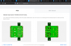
Not sure why you are having so many problems. I just went to post #512, downloaded the file there, and submitted to JLCPCB - and it accepted it no problem. The Gerber viewer shows the board correctly. I also uploaded it to Online Gerber Viewer and checked there and it works too.
So here is the link to the tested Gerber file: https://www.diyaudio.com/forums/att...plier-cap-mx-gtose-mjohnson_r1_2018-08-31-zip
You might try renaming the extension of the drill file from .txt to .drd and place in same directory - this is done in the attached file below and it works well in Gerber viewer.
I just uploaded the exact gerber file from your link to JLCPCB and it looks like the output transistors are being included as part of the PCB outline. JLCPCB is getting confused about the board outline and is including the output transistors as part of the outline and increasing the detected board size. It is detecting 124x90mm(4.9x3.54 inches).
I have enclosed a screen shot.
Attachments
Last edited:
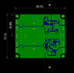
I just loaded the Gerber files in the KiCad gerber viewer and it does appear that the board is smaller than what JLCPCB is detecting. The output transistors along with two drill holes appear as part of the PCB area and then the PCB outline.
Any chance that the originator can upload a fixed version with the correct PCB outline in the edge cuts?
Edit: I have attached an image of the errors in the outline layer where you can see the outline extending beyond the PCB dimensions.
Any chance that the originator can upload a fixed version with the correct PCB outline in the edge cuts?
Edit: I have attached an image of the errors in the outline layer where you can see the outline extending beyond the PCB dimensions.
Attachments

Last edited:
- Home
- Amplifiers
- Power Supplies
- Juma's Easy-Peasy Capacitance Multiplier