scott wurcer said:Yesterday Barrie Gilbert showed me how to extend the James Schmook gm flattener to +-300mV of distortionless input range. Amazing.
OK, and that would be...?😕
Edmond Stuart said:My circuit is already balanced, as it is complementary. It is pointless to double balance this circuit. Ask Bob Cordell. 😀
At least my devices (models and in the bin) are not enough complementary, if I look at the distortion of the balanced vs. non balanced input topologies.......
Parts of the same polarity are easier to match closely, although not as close as the simulation models

At least for open loop designs or low feedback, balanced seems the way to go, measurement-wise.
Tino
zinsula said:I'm only showing what I got. Nothing to "prove".
An I tried to compare same topologies.
Your BJT topology should be compared with a similar JFET topology.
See attached schematic.
As far as I can see the emitter currents of Q1,Q2 vs the value of R2,R3 is not optimal. For minimal distortion R2=R3 = 0.5 * VT / Ie. (VT is the thermal voltage, ~26mV)
Would you try this also, please.
Cheers.
The transfer function of the complementary differential fet, PROPERLY DONE, is more linear than any single differential fet pair as the 2 separate gain stages sum the signal and subtract the even order harmonics. It has nothing to do with balance. In fact, it is easier to make a balanced circuit with just a single diff pair, but you don't get the same distortion performance, UNLESS you do the Gilbert type linearization,(with bipolars) which is not easy to do, and may generate or at least allow higher order harmonic generation.
A REAL question. IF you measure a single fet and get only 2'nd harmonic distortion. WHY does a differential FET pair have only (or mostly) 3'rd harmonic distortion? Where does the 3'rd harmonic come from? This question is also important in output stages, where there is a difference between class A and close to ideal class B. Why is this so, also? Please, try think about these questions, or else we go in circles and we cannot progress.
A REAL question. IF you measure a single fet and get only 2'nd harmonic distortion. WHY does a differential FET pair have only (or mostly) 3'rd harmonic distortion? Where does the 3'rd harmonic come from? This question is also important in output stages, where there is a difference between class A and close to ideal class B. Why is this so, also? Please, try think about these questions, or else we go in circles and we cannot progress.
john curl said:Where did the higher order harmonics go, PMA in in the 10K example?
They are more or less FFT phaseshifts results, remember their level, which is less than -150dB.
SY said:
OK, and that would be...?😕
Sorry, trade secret for now and it requires a lot of exact area ratios in any case.
OK.Edmond Stuart said:
As far as I can see the emitter currents of Q1,Q2 vs the value of R2,R3 is not optimal. For minimal distortion R2=R3 = 0.5 * VT / Ie. (VT is the thermal voltage, ~26mV)
Would you try this also, please.
Cheers.
Changed to 2.7 Ohm / 5mA Ie
I had also chosen 10 and 20 Ohms for Fet Sources mistakenly, now 10 Ohms for both N and P channel.
Attachments
john curl said:Well, DUH, Edmund! You have 2 completely different circuits. One is JUST a follower, the fet design is compromised in a BIG way with the 220 ohm bias resistor, change it to 22 ohms and run it again.
No! The bjt circuit is a CFB input stage, with an inverting and a non-inverting input. Please look better.
Lowering the resistor to 22 Ohm does improve the distortion, in fact, it's now roughly the same as the bjt stage, but the two circuit are NOT comparable any longer, as the drain currents are more then 3 times higher, DUH!
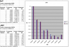
Edmond Stuart said:Pavel & Tino,
Are you proving that JFETs produce less distortion than BJTs?
If that's the case, then I'm not convinced.
The circuits below convinced me of the opposite.
They were operating at almost the same conditions.
Io = 2mApk-pk
JFET: THD20=479ppm (blue)
BJT: THD20 = 36ppm (red)
Cheers.
Edmond, it is not very good to compare input complementary-differential stage (V/I) with unity gain diamond buffer (V/V).
Edmond Stuart said:
No! The bjt circuit is a CFB input stage, with an inverting and a non-inverting input. Please look better.
Lowering the resistor to 22 Ohm does improve the distortion, in fact, it's now roughly the same as the bjt stage, but the two circuit are NOT comparable any longer, as the drain currents are more then 3 times higher, DUH!
Well - you are right. But they are really different structures, we compared BJT and JFET differential input stage, your CFB has almost zero -input impedance, and structure is well known and explored - and very good, agreed.
The case is that that CFB circuit is not well applied as a balanced, you should use 2 such circuits.
G.Kleinschmidt said:
WRT amplifier noise, it is useless to consider the effects of only the input stage when using low gm devices such as jfets for input stages. Without a high impedance drain load the gain will be low and then the noise contribution of the following stage (typically the VAS) will contribute to a greater degree. BJT’s with their much higher gm are ahead in this regard.
Cheers,
Glen
This is one of the reasons that I employed the unipolar input/VAS topology that I did in my MOSFET EC amplifier. That topology achieves a differential current source load, so the voltage gain of the unipolar JFET input stage is very high, even with the lower gm of a JFET LTP as compared to a BJT LTP. It helps me have my cake and eat it too.
I do agree with John that in general BJT input stages are more susceptible to RF EMI by way of possible junction rectification effects than are JFETs.
Cheers,
Bob
Thanks for agreeing on that, Bob. I was thinking that I had really lost my mind, when nobody else seemed to understand the situation. I'm not getting any younger!
PS You made a pretty darn good power amp, years ago. I just like my way, just as much.
PS You made a pretty darn good power amp, years ago. I just like my way, just as much.
john curl said:A REAL question. IF you measure a single fet and get only 2'nd harmonic distortion. WHY does a differential FET pair have only (or mostly) 3'rd harmonic distortion? Where does the 3'rd harmonic come from? This question is also important in output stages, where there is a difference between class A and close to ideal class B. Why is this so, also? Please, try think about these questions, or else we go in circles and we cannot progress.
Hi John,
Here is my understanding of the answer. We usually associate asymmetrical transfer functions with the production of even-order harmonics. We associate symmetrical transfer functions with the production of odd order distortion. If we take a perfectly even-order transfer function JFET and put it together with another identical one in an LTP arrangement, the resulting net transfer function of the LTP becomes perfectly symmetrical about 0. Such a perfectly symmetrical transfer function cannot produce second harmonic distortion.
Cheers,
Bob
john curl said:Thanks for agreeing on that, Bob. I was thinking that I had really lost my mind, when nobody else seemed to understand the situation.
No one? I have to laugh loudly 😀
Re: Not fair?
I don't think you necessarily changed it to make the comparison completely valid. Could you please post up the models for the jfets you are using. I'd like to have a play later when I have the time.
Cheers,
Glen
zinsula said:
With both arrangments, I have a "gm" in R1 or R11 of 3.75mS (=3.75mA per 1V input swing), and this is fair enough I think. This Gm I use to mirror the current and this will result in the same OLG.
But I have changed the arrangement:
R2 - R5 = 150 Ohm
R6 - R9 = 750 Ohm
For the same current swing, I had to set R1 = 100 Ohm.
These are the results:
I don't think you necessarily changed it to make the comparison completely valid. Could you please post up the models for the jfets you are using. I'd like to have a play later when I have the time.
Cheers,
Glen
Bob Cordell said:I do agree with John that in general BJT input stages are more susceptible to RF EMI by way of possible junction rectification effects than are JFETs.
Cheers,
Bob
Hi Bob.
I have no argument that a non-emitter degenerated BJT LTP can work as excellent AM detector (especially if Ie is reasonable, decreasing re and increasing the gain), as only a very small non-common mode AM RF signal is required to overload it.
But to repeat what I wrote in my first post on this topic (specifically referring to the input stage):
Jfet input stages have no significant advantage in this regard over bjt input stages emitter degenerated to a similar gm.
This statement isn't general, but quite specific. I think that any advantage a jfet input stage under these conditions may have over bjt input stage isn’t significant because if you have enough stray RF voltage to overload the input stage (reverse bias the b-e junctions) you’ve got other problems to worry about.
And generally, non degenerated BJT input stages are far from optimal for other reasons besides RF detection.
It does get boring when someone claims that a simple statement like the one above is wrong, and then to prove it, argues for a point that isn't under contention.
Cheers,
Glen
PMA said:That's also the case with Douglas Self's analysis of "Small signal stages". He shows distortion of the whole amplifier, no one knows at what output amplitude, no one knows what is input voltage, no one knows distortion of the isolated input stage.
That is not true and a complete misrepresentation:
http://www.dself.dsl.pipex.com/ampins/dipa/dipa.htm
An externally hosted image should be here but it was not working when we last tested it.
- Status
- Not open for further replies.
- Home
- Amplifiers
- Solid State
- John Curl's Blowtorch preamplifier