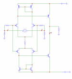
The third subcircuit is very much like the second, but with fet's, either jfet (as shown) or mosfet. This shows that the input stage is easily interfaced with about any part type..
Each approach has both advantages and disadvantages, usually due to the intrinsic flaws in the second stage devices.
For example, the bipolar second stage will give more gain, but with a slightly higher order series of harmonics due to the intrinsic transfer function of the bipolar itself. However, it can be much more 'balanced' since the output Z of the complementary bipolar devices are well matched (within reason). This is NOT so with mosfets, for example, and if you use a mosfet second stage, you WILL get more 2'nd harmonic than with a bipolar second stage, but an overall smoother (less higher order odd harmonics) transfer function.
A jfet second stage is possible exactly as shown in the third example, BUT you must take care with voltage breakdown, because each output device swings across the whole range of +/-V so with a +/- 24V supply, you should use a 50V part pair, and this is difficult to find, without losing about 20 dB of gain, due to the extremely low Gm of the 'long gate' jfet types, compared to the 'short gate' types like the Toshiba, etc.
When it comes to low noise design, I find many examples put up here, very far behind today's technology, at least 40 years behind.
Normally, we do not make MC input stages with a single bipolar transistor operating at high current. This is because of the relatively high bias current that will have to be taken care of, somehow. Cap input drives the low frequency noise up, for example.
Now, a single or paralleled jfet can be used successfully, because of the very low gate current.
Even 39 years ago, we used complementary bipolar transistors with betas matched at operating current, to cancel the overall base current, and then kept operation (even with multiple bipolars) down to 2 ma or so, to reduce the primary base current to something reasonable.
Looking at the example cited here, I find a bit behind the times.
I'm advised privately that numbers and packages have changed for the parts since the acquisition by Diodes Inc., and at least the 650/750 devices are now renamed and in SOT223 packages.
SO, my gut feeling was right, to keep them... Also, I bought recently some KT-626 on epay (Soviet PNP), despite I have no idea where I would use them...
PMA's example is very good if you want a lot of gain. However, in can be somewhat more noisy as drawn. Normally, emitter degeneration resistors would be added to reduce the NOISE GAIN of the bipolar devices.
It is just a circuit 'hint'. But it seems to be viable and can be easily modified. It has both high gain and OLG frequency as drawn, and it is very fast as well. For a gain like 40dB, very low distortion and wideband circuit can be built, with very high slew rate.
Regarding emitter degeneration resistors - the circuit has JFET input devices.
Regarding emitter degeneration resistors - the circuit has JFET input devices.
Last edited:
That won't be easy due to 2nd stage transistor's B-E junction effectively clamping voltage across current mirror.PMA's example is very good if you want a lot of gain. However, in can be somewhat more noisy as drawn. Normally, emitter degeneration resistors would be added to reduce the NOISE GAIN of the bipolar devices.
Regarding emitter degeneration resistors - the circuit has JFET input devices.
The current mirror devices, the gm is higher on the bipolars than the FET's so there is noise gain. The output has no way of defining its standing current either.
The output transistors would need small emitter resistors for this reason.
The common mode current in the output is still undefined. I posted a circuit over a year (2?) ago that overcomes both problems, I could post it again tonight. I built it and tested it to show that as claimed the input offset and Aol could be independently trimmed to 0 and infinite respectively, I think I even posted scope plots.
Borbely's last power amp used matched and parralled 2sk170 and 2sj74 jfets cascoded with 2SK2013 and 2SJ313 Fets as a 16ma VAS configured as John's Parrasound 3000 VAS. The input dual differential was cascoded 2sk389/2SJ109.
Last edited:
John,
Going back to your subcircuit #3 and using Mosfets in 2nd stage. Can one assume that, all else being equal, despite their higher capacitances the sonic advantages (less high order distortion components) of using them outweight the loss of the circuit's slew rate?
Best,
Going back to your subcircuit #3 and using Mosfets in 2nd stage. Can one assume that, all else being equal, despite their higher capacitances the sonic advantages (less high order distortion components) of using them outweight the loss of the circuit's slew rate?
Best,
The mosfets that we would normally use for the second stage would be 1/2A-1A devices, and would not have too much capacitance to work. Just look at the JC-1 power amp that uses this topology.
I might clarify what I mean by 'noise gain' or whatever it is called formally.
The first estimated example of this, I learned from a classroom handout of the UA741 op amp that had been analyzed by the best SPICE emulation at the time. It was shown that the bipolar active loads actually ADDED noise to the op amp, because they were not degenerated enough to kill their noise gain. This was a revelation to me, in 1971. I would have never thought it would be important, until it was discussed in class.
You see, we normally think of the input device(s) as the primary noise generator, because we normally use a resistive load. However, when we use an active load, then the load itself can amplify its own self noise, and sometimes overwhelm the input noise. The easiest solution is to add emitter resistors in order to reduce the intrinsic gain of the active load. However, too much emitter resistance will cause voltage drop problems that could effect the common mode range, or the maximum output swing of the circuit. This is where 'finesse' is required, to keep the potential problems almost negligible.
The common mode current in the output is still undefined. I posted a circuit over a year (2?) ago that overcomes both problems, I could post it again tonight. I built it and tested it to show that as claimed the input offset and Aol could be independently trimmed to 0 and infinite respectively, I think I even posted scope plots.
Scott I'd be interested. Can you post your circuit again?
Scott I'd be interested. Can you post your circuit again?
Sure, I need to rerun some sims for a simplified version.
Sorry, OT I know - but re '2012, our time is running out', did you see the article on NatGeo website about rogue planets that have been ejected from the core of the Milky Way at >40million Kms/Hour. One of those through our neck of the woods . . .
- Status
- Not open for further replies.
- Home
- Member Areas
- The Lounge
- John Curl's Blowtorch preamplifier part II