That also was the file I encountered just wandering through the results of a Google search for "Hood Liniac".
Another parts query.
2SJ74 amps in the PSU regulator - must these be used for low noise etc or can another amp. (there are not many p channel amplifier types apart from 2N546x series or 2n3820) be substituted?
2SJ74 amps in the PSU regulator - must these be used for low noise etc or can another amp. (there are not many p channel amplifier types apart from 2N546x series or 2n3820) be substituted?
I picked the 2SJ74 for low noise and high gain. I don't know of any other P-channel "commonly" available that will match it (at least, I don't have any). There are some old Toshiba devices that would work in its place, but I'm afraid they'd be even harder to find.
You could replace the 2SJ74s with low noise PNPs like the 2N5087. In that case, I would redce the tail current source to 2ma or so (it's currently set at 5 ma) . You could actually reduce the tail current to ~ 1ma if you wanted - the tradeoff will be between gain/drive capability and noise from the interaction of the base current with the voltage divider network. Reducing the impedance of that network would help.
You could replace the 2SJ74s with low noise PNPs like the 2N5087. In that case, I would redce the tail current source to 2ma or so (it's currently set at 5 ma) . You could actually reduce the tail current to ~ 1ma if you wanted - the tradeoff will be between gain/drive capability and noise from the interaction of the base current with the voltage divider network. Reducing the impedance of that network would help.
Last edited:
Hmm....well you did say "advanced" project, didn't you. I'll try sourcing the 2SJ74s economically but 2N5087 is somewhere in my parts boxes and ok if the noise level proves acceptable. Thanks for the suggestion and particularly the guidelines for the application. Much appreciated.
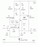
The "Liniac Inspired" circuit has been working in my living room setup for the better part of a year now - no complaints about the sound. I'm thinking of trying this variant using one of the Supertex depletion mode fets. Most likely I'll need some sort of compensation cap, but I'll find out when I fire it up. Since I don't have any models for the Supertex fets, I'll be building this one up on perf board first. It'll probably almost work with the values shown in the schematic posted here, with some tweaking for the biasing current source. Another possibility would be to use a PNP Darlington rather than the P-channel mosfet for the output circuit - the higher transconductance may give lower distortion.
Attachments
I have all the components spotted in place on the perf board. Tomorrow might see this baby all hooked up and ready to test...
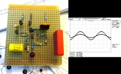
Things are easy to build on perfboard, and this ocircuit makes a fairly compact module, even with no real effort to make it compact - the board is ~2.5 X 3 inches. Attached is a picture of the breadboard and response scope picture. I'm going to need to add bypassing to get real HF behavior, but from inital observations, the circuit might need 10-20pF of compensation. I'll need to add the power supply bypass and carefully calibrate both my scope probes for flat response before I can look more closely. I can say this - the thing is fast....
Attachments
This is the latest schematic to center the output voltage and up the output fet quiescent current to 20ma. I think it'll stay this way for a while. I'll want to look at the square wave response again to set up the compensation, which will be somewhere around 20pF, I think.
Attachments
Attached are the rise and fall times of the previous circuit with a 33 pF compensation cap. It looks like the line amp is following the input without any extra garbage. The ringing on the waveform fall time is due to ringing from the source - plain and simple. Next up might be to throw it at my HP 8903 to check THD. I suspect it'll be low.
Edit - for the sake of clarity, the top waveform is the output, and the bottom is the input.
Edit - for the sake of clarity, the top waveform is the output, and the bottom is the input.
Attachments

Last edited:
I suspect that if I use a smaller output fet like the VP0106N3 or the ZVP3306A instead of the IRF510 at the output, I'd get better response due to the lower capacitance. Depending on the package, I might have to glue a small heat sink to the device.
Which part of the circuit makes it "Liniac"?
And what is it doing to "improve/change" the operation?
And what is it doing to "improve/change" the operation?
Read the posts - I'm now calling it "Liniac Inspired", as I'm sick and tired of all the quibbling that really has nothing to do with the circuit. The idea I stole from the Liniac articles (besides the basic feedback pair) was stiffening up the drain of the input device with a current source. This is all explained in the thread.
The problem this particular circuit addresses is to get a low gain buffer (gain <10) with good output centering and low distortion . A similar circuit with a current source at the source of the input device makes a heck of a unity gain buffer, and I used said buffer until I came up with this circuit. The first incarnation of this circuit is in my living room system. The second one will be possibly getting some measurements with my 8903A this weekend.
I could possibly ( make that certainly) do a circuit using
2SK170 and 2SJ74 that would work as well or better than this circuit, but the very purpose of this exercise was to be totally stubborn and eccentric and avoid doing that. Also, I was intrigued at the possibility of using one of the Supertex devices in a gain context, as nobody else seems to be using them for anything besides current sources. I used the TO-92 flavor in the circuit I just presented.
Found much of it in post59.
Judging other comments in this Thread, you may have thought I was having a dig at you.
That is not the case.
I simply wanted to know what made a "liniac", it seems the CCS load on the first and the second Darlington make it such.
Judging other comments in this Thread, you may have thought I was having a dig at you.
That is not the case.
I simply wanted to know what made a "liniac", it seems the CCS load on the first and the second Darlington make it such.
This little fit of pique on my part had one good outcome - I actually went and simulated a 2SK170/2SJ74 lineamp using small-signal Darlington outputs. The circuit is a mirrored complementary version of the basic skeleton of the one I presented here, minus the extra current sources and doodads. It took <1/2 hour to get something that balanced and simulated well. I strongly suspect that the circuit or something close to it has already been invented by someone else years ago (probably JC or Erno) - it was too easy to be otherwise.
Just to be perverse, I also ginned up a version using the J176 and J113 for input jfets, with mosfet outputs (Zetex small-signal devices). The J176 and J113 need some small helper current sources to perform at their best, which is about twice the THD of the fancy-pants Japanese solution. This is not a bad place to be for "Joe Blow" fets like the ones I used.
If someone asks me nicely, I'll post what I did in a separate thread.
These symmetric circuits also present the possibility of using an opamp servo to ditch the output capacitor. Despite violent opinion to the contrary, I use an input cap on everything, as you can't trust anything in the outside world. I have too many commercial products with DC offset on their outputs (one would be too many). I suppose I could fix them with an output cap or a little more hacking, but I'd rather spend my time building new circuits.
I did a little casual searching, and both JLH and Hiraga have some similar circuits. The JLH circuit is a unity gain buffer, and the Hiraga circuit is "Le Monstre". Hiraga cascodes his input jfets, something I was tempted to do. Maybe later...
Last edited:
Just to be perverse, I also ginned up a version using the J176 and J113 for input jfets, with mosfet outputs (Zetex small-signal devices). The J176 and J113 need some small helper current sources to perform at their best, which is about twice the THD of the fancy-pants Japanese solution. This is not a bad place to be for "Joe Blow" fets like the ones I used.
If someone asks me nicely, I'll post what I did in a separate thread.
Wrench... I would be more than grateful if you post it, I am following your threads with biggest interest for some time. Stashing the fets in the mean time...
Thanks in advance!
mad_z
- Status
- Not open for further replies.
- Home
- Source & Line
- Analog Line Level
- JLH Liniac Revisited