Hi prasi, back in post #6372 on the 30th April, you said you would post the gerber files and final layout and schematics. Are you still working on this design and when do you think you will be able to post the relevant final documentation. I would like to get some pcb's ordered as soon as you post the files, thanks.
Regards,
Gary..
Regards,
Gary..
I have a couple of comments on mjona's observations.
First, I do not think an inductive component will have any significant impact when in the position of R2-R12 - these are supposed to be a constant current source, and if anything, an inductance will help to increase the impedance and make a better current source.
I have not simulated this - I may be wrong, but with a high series resistance, (note this caveat) any inductance in a wire wound pot is unlikely to be a problem, but may actually be an advantage. A possible downside might be that a protective diode should be added to prevent damage in extreme circumstances (clipping).
Secondly, while I agree that JLH's modification using a transistor pair instead of resistors does allow the use of a low power pot, it detracts a little from his original concept in that a bootstrap circuit, though considered old fashioned now, provides a higher output voltage and can drive the upper transistor to its Vce(sat) value instead of being limited to about a volt or so below the rail (plus a Vbe drop), so if only from that point of view requires a higher power supply voltage and affords lower efficiency than his original. This is not to criticise the idea of using a CCS - most Class A builders won't really care for a slight increase in power, I suspect, but I do think the original circuit is more elegant.
The main problem with using a pot (without padding resistors) is that it will be large; it will probably be wire wound; and certainly not cheap these days.
If I were to build a JLH again I'd probably measure the device gain and use a fixed resistor as appropriate, as Nigel and Ian have mentioned. In a production environment it might be as easy to use a medium power pot just to test the setting needed - using test pins - and solder in the nearest resistor to that value, especially as it would need to be a 1W part.
I agree that pots always seem to lose performance after a few years, so I agree with the recommendations for a fixed resistor, and that is my preference over a CCS - for this particular circuit at least.
While bootstrapping increases the apparent collector load it relies on a form of feedback from the output having positive phase involving an element of a.c. It is this which allows slightly greater voltage swings than with constant current sources and slightly more power.
The bootstrapping still relies on the negative feedback doing the job of error correction at the same time and both loops originate from the output and both deal with a.c.signals. If a.c. is passed through an inductor like a wire-wound potentiometer there will be some alteration in phase the effects of which I think ought not to be recycled into the forward transfer path - however small these may seem.
The standing current in this amplifier can be flexible as long as it is near enough to meet the need depending on the power supply voltage.
While one could buy a single wire-wound pot and use this for setting up a pair of channels, the mention of an DIL 8 switch made by Grayhill raises the prospect of making a ladder switch at far less cost.
I suggest that to allow some flexibility for variations in supply voltages etc output standing current should be set to keep the output transistors case temperature below 60 degrees.
While that will depend on local climate and season such could be controlled by a thermostat with normally closed contacts - this being in series with the power supply and mounted on the same heat sink as the output transistors.
manel - here is the test circuit with the ammeter added. The current should be set to 100mA if you don't have an autoranging meter.
This determines the base current needed for the transistor to pass 3A (this current can be checked by measuring the voltage across the emitter resistor).
The base current is therefore needed in the circuit to drive the upper output transistor at full current. That is set by R1 and R2 (plus any other series resistor like R12 in Prasi's diagram).
You need to add a small margin so that the driver transistor does not cut off completely.
That would be something like 10-15% extra, but any increase has a direct impact in output dissipation, and standing current, of course.
In Prasi's circuit if the base current of the MJL21194 is 50mA, say, then adding 10% means 55mA in the resistors. The supply voltage is 24V so the voltage across the resistors is half this, less a Vbe of the upper output transistor, or about 11.4V.
That makes the resistances needed total 11.4/55mA=207 ohms. These can be split 50:50 but reducing R1 generally helps. In Prasi's circuit R1 is 47 ohms, and R2+R12 is the remainer at 160 ohms, though probably the 10 ohm is not really necessary - but the output stage current will increase a little if omitted.
Thanks John, I think I will understand. I will have to study it carefully though. I am very new to the subject. I have built the 1969 JLH and it works fine, but I think I could improve it if I manage to do some fine tuning.
Thanks again.
Manel.

I said I would draw this. It is a safe 10 minute experiment. It will make the JLH able to be driven by a CD player. A 20 K log pot to control the volume, 10K should be OK if that's the choice.
???? Is where a similar double value might work. The 220R is just soldered on top of the one on the PCB as in red dots ( solder ).
There should be very few disadvantages to this. A tiny bit more hum and hiss. It might sound nicer! I suspect tuning this is more important than buying high speed transistors. If you use less gain ( 470 K ? ) an oscilloscope must be used. TIP2955 TIP3055 as a reference transistor if 1.2 A standing current. I admit 30 MHz devices are sometimes cheaper. Higher gain suits the 30 MHz devices as they can cause marginal stability, high gain wins back some stability margin.
As always there seems to be never ending opportunities for discussion!
Regarding mjona's point about bootstrapping, of course it is the ac feedback which drives the voltage above the rail. Bootstrapping provides positive feedback, but at a gain dependent on the output transistor(s). In the JLH original circuit the gain is about as high as it could be, with no emitter degeneration/current limiting resistor, close to 0.99 for a small signal - but less, as this is a large signal situation, so likely to be more like 0.95.
Due to the bootstrap feedback, the presence of a small inductance will have very little effect if any on the gain and phase. I would agree that if the inductance were large it would affect the gain: phase relationship, but the inductance of a wire wound pot is unlikely to be much greater than 100uH - I haven't found any manufacturer's data on this.
The idea of using small DIL switches that I mentioned does seem to be a cheaper option. ANd allows for transistor replacement (should the need arise) without having to readjust a fixed resistor.
My concern about the bootstrap is from a different perspective. That is, the feedback is dependent on the output transistor, and if that is slow, (like the old 2N3055H) the rise time is severely slew limited. That slew rate is much better for faster transistors, and if a constant current source is used, which (negative feedback) helps to pull the devices up more quickly.
But with fast transistors (30MHz) this problem seems to be addressed.
If, owever, you are going to go to the trouble of adding transistors to make a constant current source, it seems to me to detract from the original concept. Why not go for broke with a fully complementary output stage and differential input?
I've answered this too, in various posts - in the basic form it does not work! The overall distortion is higher, and analysing that reveals that the second harmonic distortion in the input stage counteracts some of the gain reduction in the output stages. Which is a subtle advantage of JLH's original design. But then, increasing the gain as Self showed with a Darlington (or emitter follower, if you prefer) and using active current control would avoid the need for trimming pots at all.
And finally, Nigel raises another interesting point. In JLH's article he mentioned an open loop gain of 600. I fear that he (JLH) may have overlooked the effect of the 220 ohm "grounding" resistor in the feedback loop. This adds to the input transistor emitter impedance, which works out at around 75 ohms, totalling 290. Using that as the input stage gain,(3.4mA/V) and a driver/output transistor gain of 100 each leads to something in the region of 250.
Nigel's proposal to halve the feedback resistor will probably have little effect on the distortion, because the OLG will increase almost as much as the closed loop gain.
If you are talking about the addition of a second resistor of 220R in parallel with the "to earth decoupling leg of the feedback divider" in Nigel's recent post, whether or not this will have as little effect on distortion as you might assume may not be in line with what others may aspire to.
To put some context around this proposal, that will increase the closed loop gain to roughly double and reduce the feedback factor by roughly the same amount.
One might get away with this in a more complex amplifier with a large unity gain bandwidth product, which may be regarded as working capital. For me with around 30 dB in this circuit the reduction in feedback and the prospect of increasing distortion is not easily dismissed.
That said it some parties have replaced 2N3055's with super beta transistors like MJL3281 which would increase the unity gain bandwidth product which would allow some modest increase in closed loop gain. At present these have lead capacitors in the feedback loop to reduce the closed loop unity gain frequency to ensure stability. An increase in closed loop gain has the same effect.
Last edited:
Bootstraps are fantastic.Positive feedback between 50 and 97 % works well. Above 93 % a small resistor in the feedback loop help's. Square waves show trouble above 93%. I doubt that the JLH can go that far. Complimentary feedback pairs might. I never saw a bootstrap on a valve amplifier apart from what I built. It works amazingly well if you do. Input bootstrap works well.
To put some context around this proposal, that will increase the closed loop gain to roughly double and reduce the feedback factor by roughly the same amount.
I was referring to Nigel's suggestion of halving the feedback resistor which goes to ground, which I often refer to as the "grounding resistor".
I think you may have missed my point that the open loop gain will increase by almost double?
Therefore, the loop gain is almost the same as it was before the change, so there will be little change in distortion.
Not quite, the distortion will increase a little because the open loop gain is not increase by exactly 2 but more like 1.6.
That could be restored if the PNP input transistor current is increased to 800uA to 1mA, but that would need a current mirror or something to replace the 8.2k resistor (while maintaining the gain).
Regarding the bootstrap - I think if you calculate the phase of the current entering the bootstrapped resistor, it will appear inductive. Therefore, a (small) inductor in series with R2/R12 should have little effect on the overall performance.
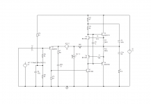
I am attaching an off the cuff simulation of the original Class A circuit. This uses devices from the LTSpice library - the 2N3019 is a version of 2N1711. I had to play with the bootstrap resistor values to get 1.2A of output standing current.
Transistor .models assume working at room temperature (25 degrees C) but when the outputs heat up the standing current will increase. I have done a test on my 1996 Class A amplifier where the room temperature was 18 degrees C.
The standing current measured across the CCS resistor 0.33R dropped 0.51 volts settling to 0.55volts after 15 minutes a variation between 1.55A and 1.67A. In summer the start and finish posts move.
We are out of summer now however I remember the voltage drop getting up over 0.6V at the end of warm up. The heat sinks are rated at 0.3 degrees per watt of heat dissipation. There are two of these one for each channel.
My 1996 amplifier uses 2N1711 and 2N3055 devices albeit it uses the constant current replacement of the bootstrap. If the value of RV1 is left at 100R it may result in enough current for driving 4R loads if the outputs get hot enough.
I looked at some wire-wound potentiometers sold by RS Components which would cost more than a couple of super-beta transistors while the power rating is only 2W. You could get the same from pairing 1W carbon film resistors.
I have included a link to Bob Cordell's website in case MJL21194 or other selections from his collection are of interest as substitute parts. It is worth looking at the FFT graphs using start times of 4ms for 1kHz testing and 200us for 20kHz.
It will be seen looking at Ie via the View Visible Traces icon on the toolbar - that although the output stage standing current is 1.2A this is not constant and the peak currents are greater than this.
Attachments
Isn't it incredible how much can be written about this seemingly simple amplifier.
Another simple idea worth trying is a 22 uF 100 V polyester in parallel with the output capacitor. This was a typical 1980s modification. These days electrolytics are better so possibly not as noticeable. With a little imagination that capacitor can be the tweeter capacitor. Draw the circuit if so of the loudspeaker. The 0 V and tweeter plus must be isolted from the bass circuit. You don't want DC through the drive units. If the capacitor in the speaker is 10 uF polyester it most likely is suitable. My hunch is anyone who can draw the crossover will be able to do this. A bit like motor vehicle repairs one has to have belief in your own abilities.
Tweeters can be wired with thin wire to give a more open sound. This ideal biwiring in my own system using Quad 303 got rid of my only doubt about the 303. The system had a more modern sound. The modification cost me mostly my time.
I do not disagree with mjona's results. I have simulated the original JLH with both gain variants and it is in line with my previous post. Which is to say that if the closed loop gain is 2x and the open loop gain 1.6x higher, then the distortion I would expect to see is 2/1.6 times greater. The increase is as you woudl expect from a reduced linearity in the PNP input device.
As regards the 2N3055, that depends on the model. I found no models for the original 2N3055 (RCA hometaxial), most describe an epi device. Using my own model it is easy to see the problem with the frequency response. In a simple circuit like the JLH at 20kHz the transistor turning off doesn't, at least not quickly enough, so the one turning on has to compensate by increasing its current above what it would like to. ANd that is the problem. In the JLH original, there is no more base current available than the bias current allows. In a circuit with driver transistors, there is a chance that the drivers can increase the drive current. So, that is in essence why fast transistors are a better choice than the 2N3055H. I did not see any problems using a 2N3715 transistor (4MHz epi) at 20kHz.
Regarding the modified '96 circuit, I would have thought that builders would have put the current monitoring transistor of the CCS on the heatsink of the output devices to provide a degree of thermal compensation?
Last edited:
To be fair, JLH originally specified MJ480 or MJ481 devices. These are actually a very good choice as they were not only 4MHz but also have low capacitance junctions. The 2N3715/16 devices were an excellent choice for higher powers (but more expensive).
The 2N3055 came later, I think after a lot of people started using them. The modern equivalent epi device should be superior to the old RCA device - except at low voltages when quasi-saturation will reduce the gain!.
The MJ(L)21194 devices have better current gain characteristics but the junction capacitances are rather large which implies more drive current is needed at higher frequencies. That MAY risk high frequency problems again -that would be worth investigating.
1W carbon resistors do seem a better choice than a WW pot, not only because they are cheaper (by a big margin) but also for better long term stability, even if they have to be trimmed. I'm sure there would be some who would want a pot to adjust the JLH though!
I would suggest 1W resistors too, over parallelling 1/2 W resistors. I have found that modern resistors seem to have become physically smaller than older generations of 1/2W resistor. In some recent circuits, two 1/2W components became hotter than a 1W replacement.
It is as though all manufacturers are relying on some form of heat dissipation in the PCB to get rid of excess heat. That only works to a limited extent, and cannot be ignored if several components are aslo expecting heat to be removed in the PCB - that can only handle a small amount. The 1W resistors have a bigger surface area which may help.
Except, though, the idea of using (up to) 8 resistors in parallel with the switch approach, means there would be probably at least three resistors in parallel if higher currents were required, spreading the heat load out between more of them.
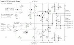
Why not go for broke with a fully complementary output stage and differential input? .[/QUOTE said:John why not fully complementary output power stage but with original JLH singleton input stage ? (#4304) JLH 10 Watt class A amplifier
That is an option. There are some definite advantages in such a scheme. My suggestion is to use a couple of transistors to set the bias automatically. The driver stage current can then increase, allowing for more overdrive than in the original design. However, the downside is that it needs a bigger current in turn. The input stage device current has been increased in the attached circuit to about 1.5mA. That gives a higher gain compared with JLH's design running at about 350uA. A further consequence is that the feedback current needs to be larger, so the feedback resistor is reduced to 560 ohms and the grounding resistor to 47.
Because of the higher current in the input stage the base bias arrangement is changed which should set the centre rail to a little above 15V.
There are some disadvantages. One is that complementary devices have slightly different IV characteristics, so this output stage will not compensate for second harmonic distortion in the same way as an NPN only pair. With modern devices which are designed to be closely symmetrical this may not be a big issue.
The circuit may not be as stable as the original, but a Tian probe suggests it is in fact almost as good with 60 phase margin and at least 40dB gain margin.
Not tried this but it looks promising. My earlier thoughts were to use a differential input for DC coupling, and a Darlington driver with current mirror to improve the gain and reduce distortion at least an order of magnitude.
Another disadvantage is that the use of emitter resistors will limit the maximum output voltage. JLH's original design was very close to ideal in that the transistors could saturate, perhaps providing an output to within 1V of the rails. This circuit will need at least 3V higher supply voltage on each side (6V for single ended output) or more.
I do like the idea of not having any pots to adjust.
Attachments
John
I think that your design is on very good track to be A-class amp par exellence ,simple and effective same as JLH 1969 amp.
I like that idea of using a pair of transistors to set the bias current automatically ,
and IMO when those pair are attached to the main heatsink altogether with 3715/3792 power pair thermal stability will be very good ,actually IMO much better than in JLH 1969 amp ,
have some NOS TO-3 Motorola 3055/2955 pairs and I want to use them to make one pair of amps based on this simple design , need about 15W for 16-ohm very efficient loudspeaker .
edit , IMO two emitter resistors 0R39 will ensure stability of the amp and is good to be there , regardless if B+ supply must to go up for several volts .
Last edited:
John Ellis' Complementary Circuit
If your 16 Ohm speaker is that efficient it may be possible for you to use John's design without increasing the supply rail voltage. Alternatively you could build two stereo pairs and connect each stereo unit in bridge formation.
The standing current of the output stage is high at nearly 1.8 A - within reason the circuit could be used with 4 Ohm speakers.
With 8 Ohm speakers in mind, I drew the circuit up in SPICE to see some THD results.
John mentions some differences between NPN and PNP transistors - this is due to the properties of the materials used to dope silicon to enable conduction in N and P regions. In this circuit Class A running seems to have smoothed over whatever residual differences between a single pair of outputs.
I used MJL21193/21194 which are claimed to give 0.8% THD unmatched and 0.08% matched - see On Semiconductor data sheet for test details. The simulation file is attached.
The distortion profile of John's circuit is monotonic and pretty uniform in pattern - that does not always follow when there are driver transistor sets to be matched as well.
John
I think that your design is on very good track to be A-class amp par exellence ,simple and effective same as JLH 1969 amp.
I like that idea of using a pair of transistors to set the bias current automatically ,
and IMO when those pair are attached to the main heatsink altogether with 3715/3792 power pair thermal stability will be very good ,actually IMO much better than in JLH 1969 amp ,
have some NOS TO-3 Motorola 3055/2955 pairs and I want to use them to make one pair of amps based on this simple design , need about 15W for 16-ohm very efficient loudspeaker .
edit , IMO two emitter resistors 0R39 will ensure stability of the amp and is good to be there , regardless if B+ supply must to go up for several volts .
If your 16 Ohm speaker is that efficient it may be possible for you to use John's design without increasing the supply rail voltage. Alternatively you could build two stereo pairs and connect each stereo unit in bridge formation.
The standing current of the output stage is high at nearly 1.8 A - within reason the circuit could be used with 4 Ohm speakers.
With 8 Ohm speakers in mind, I drew the circuit up in SPICE to see some THD results.
John mentions some differences between NPN and PNP transistors - this is due to the properties of the materials used to dope silicon to enable conduction in N and P regions. In this circuit Class A running seems to have smoothed over whatever residual differences between a single pair of outputs.
I used MJL21193/21194 which are claimed to give 0.8% THD unmatched and 0.08% matched - see On Semiconductor data sheet for test details. The simulation file is attached.
The distortion profile of John's circuit is monotonic and pretty uniform in pattern - that does not always follow when there are driver transistor sets to be matched as well.
Attachments
Member
Joined 2009
Paid Member
that is a very interesting tid bit about matching devices for hfe, in their test circuit the source impedance is 50R and the load 8R.
Last edited:
- Home
- Amplifiers
- Solid State
- JLH 10 Watt class A amplifier