 This is the most beautifull amp I've ever seen!
like it, looks kinda Pathos like.Nice craftmanship too, is this MDF with piano gloss finish and veneer?
mdf
yes, the black sides are made of MDF, but the piece on the top is made of purely lead, then veneered..
Greets,
Ralf
Luke said:like it, looks kinda Pathos like.Nice craftmanship too, is this MDF with piano gloss finish and veneer?
yes, the black sides are made of MDF, but the piece on the top is made of purely lead, then veneered..
Greets,
Ralf
*edit*
(Having just read a page back)
The top that looks like some nice slabs of hardwood with compound mitre cuts is actually veneered lead? Or did I misunderstand one of the posts?
Do you have any in-progress photos? I'd love to see how you mounted the parts inside.
eL
(Having just read a page back)
The top that looks like some nice slabs of hardwood with compound mitre cuts is actually veneered lead? Or did I misunderstand one of the posts?
Do you have any in-progress photos? I'd love to see how you mounted the parts inside.
eL
...
yes it`s veneered lead,
no in the moment i dont have pics of progress.
But soon i will build my next pair, and i hope to make some pics of the progress and the inside..
greets,
Ralf
yes it`s veneered lead,
no in the moment i dont have pics of progress.
But soon i will build my next pair, and i hope to make some pics of the progress and the inside..
greets,
Ralf
Re: ...
And the purpose of the lead is....? Don’t tell it’s to damp the vibrations.
Excellent craftsmanship otherwise.
cheers,
Argo
ralf said:yes it`s veneered lead,......
greets,
Ralf
And the purpose of the lead is....? Don’t tell it’s to damp the vibrations.
Excellent craftsmanship otherwise.
cheers,
Argo
lead
...since i build this JLH for a friend of mine, who thinks, that by dampening the vibrations of the amp will better the sound quality - i constructed these lead`s
my personal opinion is, that this lead doesnot influence sound.
But it enhances the design of the amp- in my opinion.....
Ralf
...since i build this JLH for a friend of mine, who thinks, that by dampening the vibrations of the amp will better the sound quality - i constructed these lead`s
my personal opinion is, that this lead doesnot influence sound.
But it enhances the design of the amp- in my opinion.....
Ralf
DC offset
Hi
Ive been working on this for 6 months off and on, and the first mono block fired up first time tonight.
I have built the fig 1.
http://www.tcaas.btinternet.co.uk/jlhupdate.htm
version and have +- 20V rails regulated. Quiescent current is 2.4A and I have 4 unmatched 13003 outputs.
Everything seems fine and it plays music except DC offset is 2V and MUR860 are too hot too touch. The 2 K pot makes no difference to the offset and I have searched this thread but cant find a relevant post. Can anyone suggest a fix for this offset?
Any help appreciated
🙂
ab
The best method I employed is to use two multimeters at once when setting the bias and trimming the DC offset.
One meter connects across R10 in your case.
One meter connects across speaker output.
Adjust RV1 and RV2 both a little at a time. You will then see a pattern when turn the trim one way of RV1 say the reaction of the two multimeters change accordingly. The you adjust RV1 a bit ..RV2 a bit..and keep repeating....
Must do it very very slowly, use the reading on the meters to control the number of turns of VR1 and VR2.
Good luck.
Actually I found this two CCS updated version is so much easier and steady when adjusting the DC offset and Iq setting than all the prior versions.
Regards,
Chris
Re: DC offset
Luke
You say you have followed the schematic shown in Fig 1 but then mention that you have used four output transistors, which would mean including the current-sharing 0R1 emitter resistors as shown in Fig 3. However, I assume that you have fitted the dc blocking capacitor (C4) in the feedback network.
If your connections for the Q5/Q6 ccs are correct, you should have no problems setting the output dc offset to near zero. I have had a couple of reports of this ccs becoming unstable and oscillating (which could prevent the output offset from being adjusted) but this has only been when C4 has been omitted and the ccs has to supply a much higher current.
You haven't indicated whether you have used the transtor types shown on the schematic or substitutes. In either case, I suggest that first off you check that the e,b,c connections of Q5 and Q6 are correct. If this proves to be so, and you have used the 2SA970 in these positions, you could try changing Q5 and Q6 to a slower transistor such as the MPSA56 (unfortunately not pin compatible, so a bit of lead twisting will be necessary) to see if this solves the problem.
Please feel free to email me, either using the button below or via my website, if you would like to discuss this problem in more detail.
Geoff
Chris and Geoff,
thankyou for your replies.
Chris, I had no adjustment on offset so the problem was not about getting it right, it just made no difference.
Geoff, your reply was very helpful and I went about desoldering some mpsa56 off some old pcbs I keep for spare parts.
While trying to trace out the new pin outs I noticed that a jumper from Q5 base to VR1 was missing, the fix was to solder in the jumper.
Since then Ive had other issues, I blew up my regulators and spent the day doing walks and shopping with the wife so had no time to do what I really want😎
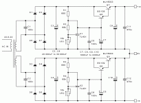
My amp uses 4 MJ15003 and 2watt 0.1 ohm resistors.
Q8 is 2SA1358, Q3 is 2SC3421 all the rest are 2SA970.
I am using C4.
Im not sure my diodes are going to cope and suspect they will cook, doesnt it seem odd that to220 diodes with a sink get so hot on 2.5A bias current?
Perhaps I have calculated it incorrectly.
I measured 0.12V drop across both R14 and R16 so its 0.12/.1 = 1.2A for each pair of transistors times two pairs approx 2.5 amps total.
Also not sure why R13 and R15 are getting so warm and R14 and R16 are not? It seems to me that they both carry the same current so should both be dissipating the same amount of power?
Heres what I get
P=I2R
I is half the total Bias, 1.25 A (Measured by volt drop across
R= 0.1Ohm
Dissipated power should be
1.25 X 1.25 X 0.1 = 0.156 watts?
Where am i going wrong here?
BTW Geoff , thanks for the good work on your website, its made this project achievable for all DIYers.
Arthur
thankyou for your replies.
Chris, I had no adjustment on offset so the problem was not about getting it right, it just made no difference.
Geoff, your reply was very helpful and I went about desoldering some mpsa56 off some old pcbs I keep for spare parts.
While trying to trace out the new pin outs I noticed that a jumper from Q5 base to VR1 was missing, the fix was to solder in the jumper.
Since then Ive had other issues, I blew up my regulators and spent the day doing walks and shopping with the wife so had no time to do what I really want😎
My amp uses 4 MJ15003 and 2watt 0.1 ohm resistors.
Q8 is 2SA1358, Q3 is 2SC3421 all the rest are 2SA970.
I am using C4.
Im not sure my diodes are going to cope and suspect they will cook, doesnt it seem odd that to220 diodes with a sink get so hot on 2.5A bias current?
Perhaps I have calculated it incorrectly.
I measured 0.12V drop across both R14 and R16 so its 0.12/.1 = 1.2A for each pair of transistors times two pairs approx 2.5 amps total.
Also not sure why R13 and R15 are getting so warm and R14 and R16 are not? It seems to me that they both carry the same current so should both be dissipating the same amount of power?
Heres what I get
P=I2R
I is half the total Bias, 1.25 A (Measured by volt drop across
R= 0.1Ohm
Dissipated power should be
1.25 X 1.25 X 0.1 = 0.156 watts?
Where am i going wrong here?
BTW Geoff , thanks for the good work on your website, its made this project achievable for all DIYers.
Arthur
Arthur, what are you using for your power supply regulators?
Geoff had suggested to me some time ago that a CCS-driven resistor was better than a Zener, so I'm thinking of using that.
(Yes, Geoff, my JLH is still in progress).
Geoff had suggested to me some time ago that a CCS-driven resistor was better than a Zener, so I'm thinking of using that.
(Yes, Geoff, my JLH is still in progress).
Luke said:Where am i going wrong here ?
I would guess that there is some oscillation going on.
If it is, a 100p cap from collector of Q3 to the emitter of Q4 should stop it.
If it is oscillating and the above does not cure it you could try 10 - 20pF from base to collector of Q3
You may not want either ( or both ) of these as a final solution but it may be a useful diagnostic tool.
I'm sure Geoff will know a more elegant cure
Good luck
Mike
Oscillation
> Is it possible that the amp is oscillating but sounds ok?
Yes, and I speak from experience. Not that you like to put your speakers through the ordeal (I had 2MHz, 3V pk-pk; and the music was just fine).
The cure (for me at least) was equally simple, just load the output with an additional 22 ohm 10W resistor to ground. The amp does not like load with very high impedance at high frequencies, which was what caused the problem in my case.
Hope this helps. But maybe it is something else.
Patrick
Arthur,
I am definitely not any expert but your regulator looks kind of strange regarding the negative rail part ???
Argo
I am definitely not any expert but your regulator looks kind of strange regarding the negative rail part ???
Argo
Arthur
Assuming you have now been able to set the output dc offset voltage to near zero, the most likely cause of a difference in temperature between the 0R1 resistors in opposite halves of the circuit is, as Mike quite rightly says, oscillation.
The 'cures' suggested by Mike will work in all probability, but it would be better to see if the cause can be resolved first, because this circuit should not become unstable if the physical layout is correct. I suggest you review the following:
1 Is there sufficient segregation and clearance between the input stage/wiring and the output stage/wiring? A physical separation of 2 to 3 inches (50 to 75mm) is usually adquate.
2 Are the connections to the MJ15003s as short as possible and are the e,b,c leads to each transistor twisted together, or at least tightly grouped, so that the formation of a loop is avoided.
3 Are the main heatsinks earthed (grounded), assuming you have isolated the output transistors, so that they do not act as aerials for the output signal.
4 Are the +/- leads from the power supply twisted together, preferrably in conjuction with an earth (ground) wire.
When you are happy that you have obtained the best possible layout, and neatest wiring, recheck the amp. If there are still indications of possible oscillation (perhaps even above the bandwidth of your 'scope), try adding an output Zobel of 10R+100nF. This is similar to Patrick's suggestion.
If the Zobel doesn't solve the problem then it is time to take action along the lines Mike proposed, though you may need capacitors up to twice the values he has suggested. Treat this as a last resort and start off with low values, increasing them as necessary until the oscillation ceases.
Your overheating diodes could well be due to the oscillation so it would be as well to cure this first and then see if there is still an overheating problem before looking for a cure.
Geoff
argo said:I am definitely not any expert but your regulator looks kind of strange regarding the negative rail part ???
Argo
It does look a bit odd, doesn't it. I don't know how Arthur came by the schematic (I have no recollection of any email correspondence with him) but it is one I prepared for a specific purpose. That was to meet the needs of someone who wanted a 'follower' type regulator as a drop-in replacement for the LM338 in the 'updated' power supply circuit. It also suited another correspondent who required a 'follower' regulator but only wanted to use MJ15003 pass transistors.
It is not a circuit I would recommend for a new build. For new work I would suggest inverting the +ve half to the circuit to form the -ve half, obviously changing the transistors to pnp types.
Geoff
HI all,
thanks for all your help, this is going on the back burner now for a few weeks, I have some kind of nasty virus and soon to be on my honeymon for 6 weeks. but you have all given me some good clues to work on.
Argo and Geoff,
I used this regulator because I had mj15003 and devilh@ck had a pcb for it on his website (BTW thanks for pcb devilh@ck)
http://www.diyaudio.com/forums/showthread.php?threadid=24320&highlight=
Geoff,
yes , I used this pcb rev e
http://www.xs4all.nl/~cfw/amp/
wiring is kept separate.
yes Im using a wire that is allready twisted, 3 strands.
One side the wires are 200mm the other side is 250mm, the main pcb is off centre on the back panel.
I need to try this, hopefully it will make the difference, I also will try to earth the back panel which the main pcb is mounted on.
no this is not done, I will try tidy this up.
if this doesnt work I will try zobel then caps accross the transistors.
mike and Patrick,
I will try your suggestions if the above fail.
thanks all for your help🙂
thanks for all your help, this is going on the back burner now for a few weeks, I have some kind of nasty virus and soon to be on my honeymon for 6 weeks. but you have all given me some good clues to work on.
Argo and Geoff,
I used this regulator because I had mj15003 and devilh@ck had a pcb for it on his website (BTW thanks for pcb devilh@ck)
http://www.diyaudio.com/forums/showthread.php?threadid=24320&highlight=
Geoff,
1 Is there sufficient segregation and clearance between the input stage/wiring and the output stage/wiring? A physical separation of 2 to 3 inches (50 to 75mm) is usually adquate.
yes , I used this pcb rev e
http://www.xs4all.nl/~cfw/amp/
wiring is kept separate.
2 Are the connections to the MJ15003s as short as possible and are the e,b,c leads to each transistor twisted together, or at least tightly grouped, so that the formation of a loop is avoided.
yes Im using a wire that is allready twisted, 3 strands.
One side the wires are 200mm the other side is 250mm, the main pcb is off centre on the back panel.
3 Are the main heatsinks earthed (grounded), assuming you have isolated the output transistors, so that they do not act as aerials for the output signal.
I need to try this, hopefully it will make the difference, I also will try to earth the back panel which the main pcb is mounted on.
4 Are the +/- leads from the power supply twisted together, preferrably in conjuction with an earth (ground) wire.
no this is not done, I will try tidy this up.
if this doesnt work I will try zobel then caps accross the transistors.
mike and Patrick,
I will try your suggestions if the above fail.
thanks all for your help🙂
- Home
- Amplifiers
- Solid State
- JLH 10 Watt class A amplifier