@Berlusconi
I'm sure you are right about the welding. I was informed by an experienced metal fab guy that alu welding is possible. They had all the kit to do it, and I believe had done exactly that for one amp builder.
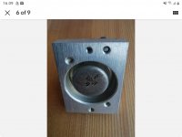
Regarding the angle, 3mm seems fairly common round here but 6mm needs to be purchased from specialist metal stockists. Putting two L's to make a T does need thermal compound between the two to make it work. Perhaps even the new graphite sheets with high thermal conductivity. Putting a T onto a flat base heatsink also needs thermal compound.
I'm sure you are right about the welding. I was informed by an experienced metal fab guy that alu welding is possible. They had all the kit to do it, and I believe had done exactly that for one amp builder.
Regarding the angle, 3mm seems fairly common round here but 6mm needs to be purchased from specialist metal stockists. Putting two L's to make a T does need thermal compound between the two to make it work. Perhaps even the new graphite sheets with high thermal conductivity. Putting a T onto a flat base heatsink also needs thermal compound.

@john_ellis
First, I do indeed appreciate your indespensable contribution to this conversation.
I am a hobbyst welder for about 10 years and I enjoy it very much. Go once to the specialised shop (warehouse) for welders and you might get many ideas. Good welders are very special people, proud of their skills. It is amazing what is possible to do with welding machine. I have a beautiful fence around my house made of aluminium S profiles.
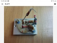
Regarding M3 screws for aluminium you're absolutely right. I have learned it hard way: after several attempts to fix transistors I have realised that M3 taps are a recipe to make Swiss cheese from heatsink. Since that first attempt I use aluminium plates to mount transistors with ordinary M3 bolts and nuts and then fix the plate on the heat sink with M5 screws.
First, I do indeed appreciate your indespensable contribution to this conversation.
I am a hobbyst welder for about 10 years and I enjoy it very much. Go once to the specialised shop (warehouse) for welders and you might get many ideas. Good welders are very special people, proud of their skills. It is amazing what is possible to do with welding machine. I have a beautiful fence around my house made of aluminium S profiles.
Regarding M3 screws for aluminium you're absolutely right. I have learned it hard way: after several attempts to fix transistors I have realised that M3 taps are a recipe to make Swiss cheese from heatsink. Since that first attempt I use aluminium plates to mount transistors with ordinary M3 bolts and nuts and then fix the plate on the heat sink with M5 screws.
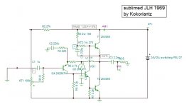
Chinese comrades discuss the JLH1969 mod using Darlington. Class AB or A.
HIFIDIY??-JC2012????????????????JLH1969 Hi-Fi?? - Powered by Discuz!
HIFIDIY??-JC2012????????????????JLH1969 Hi-Fi?? - Powered by Discuz!
A BD139-10 or BD139-16 should work as well as a 2N1711, or better.
Has anyone with a 2N1711 able to plot its output characteristics?
The Motorola Small Signal Transistor Handbook page for 2N1711 says refer to 2N3019 for graphs. The latter is in the onboard Spice Library.
I found a JLH .asc file on the internet and after a few adjustments I have basic Vout and THD simulation results. It is just a rough start to get going with LTSpice today. I will later update to match a real board I have.
Does anyone have an example of stability analysis with LTSpice?
Here are some suggestions:
-Try playing with relation between R1/R2 and plot the currents of upper and lower output transistor but keep Iq the same. Tuning for better current sharing reduced distortion significantly for me even in real life. Also improves 'efficiency', you get more current out relative to the Iq of the amp. Also check distortion FFT to see what happens.
- Check the same currents at LF while adjusting the capacitance of the bootstrap cap. Try increasing their values and see what happens to the currents in the output devices when doing this. More capacitance on the bootstrap improves the current capability/efficiency in the low frequencies.
-Input LF sine bursts and look at what happens when the burst stops/starts, tune(increase) input cap and feedback cap to see what happens.
-If you have a output cap, it needs to be of very high value not to react with the impedance of the speaker at LF.
I have increased all cap values x10 or more, and it definitely gives tighter bass.
-I posted some stability simulation of my PNP version here a couple of weeks ago. Look at Sandro's tutorial for help how to configure it for your NPN. 3.2. Measuring Loop gain and Open loop gain in LTSpice - Audio Amplifier Design Fundamentals - YouTube
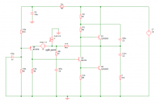
I don't have an LTSpice setup but here is a possible configuration for running a Tian probe.
The component values are set for mid rail (the 39k bias resistor is now 27k) and 1.25A (R2=270 ohms) for the 2N3055 models used.
I'm sure that the video Rallyfinnen refers to will go through the details. Essentially run two sims, first with the voltage set to 1.0, measure the voltage at the split point V1 and current through it, I1; then set V to 0 and the current source to 1.0 and run sim # 2.
Measure the voltage again, V2 and the current through the voltage source I2.
LTspice will perform the calculation - given in the Tian paper or in a slightly more readable form in one of the explanation papers others have presented.
What I do is to run the calculation with a separate program and plot the result in Excel.
If you do that note that the voltages and currents are complex numbers because of phase.
Attachments
The 2N3019 is a good device for the JLH amplifier I suspect.
It is still available from Farnell under the Multicomp banner, but who manufactures it I don't know. Perhaps Central Semi.
I have long thought that the 2N3019 and 2N4033 would be suitable for direct replacements for the 40361/40362 devices specified by Bailey for his 30W amplifier.
I have a few. Measured capacitance Cjc of a 2N3019 at zero bias is 15pF. BD139 45pF.
Although better it suggests quasi saturation might be a problem, but that might not be significant at the 10-20mA or so used in the JLH 10W.
Didn't see the output characteristics in a copy of the motorola book. will measure Early voltage sometime soon.
I don't have an LTSpice setup but here is a possible configuration for running a Tian probe.
The component values are set for mid rail (the 39k bias resistor is now 27k) and 1.25A (R2=270 ohms) for the 2N3055 models used.
I'm sure that the video Rallyfinnen refers to will go through the details. Essentially run two sims, first with the voltage set to 1.0, measure the voltage at the split point V1 and current through it, I1; then set V to 0 and the current source to 1.0 and run sim # 2.
Measure the voltage again, V2 and the current through the voltage source I2.
LTspice will perform the calculation - given in the Tian paper or in a slightly more readable form in one of the explanation papers others have presented.
What I do is to run the calculation with a separate program and plot the result in Excel.
If you do that note that the voltages and currents are complex numbers because of phase.
I did sim on Tina the JLH. The 2N3055, I have two models. The Motorola gives 1.5A bias with the given values, so I took a standard model with 1.2A.
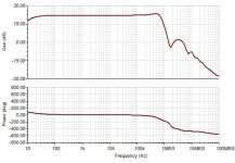
I would like to note that at 9W the distortion is 1% at 1khz. It is advertised to be 0.05% 1khz -10khz to 9W , at 5W 1khz is 0.06% but 0.12% at 10khz.
Attachments
Last edited:
I have also seen higher distortion figures than "it says on the tin".
First of all have you checked the models? If not try running some simple 1 transistor test circuits for output characteristics and fT etc. and see whether they look sensible. Are the Motorola models by MODPEX by any chance? Those are, how shall we say, not ideal.
Have you tried reducing the time step in the simulator? Distortion should reduce until some limiting value which may be nearest the truth it gets to. I usually find something in the order of tens of ns is needed for 20kHz and a bit longer is OK for 1kHz etc.
Given all that, then check the current between the two output transistors. With the old transistors the gain dips at about 300mA and as a rule (2N3055 epi especially) it needs rather higher currents but too high and the gain falls off the other side so distortion goes up again. Around 1.25-1.35A seems optimum for those devices. Ideally the currents should look similar but 180 degrees out of phase.
And also check the driver current. Inside the loop, distortion is higher, and that may show signs of clipping. I normally have to increase the supply voltage to offset that as well as optimising the current.
In real life quasi-saturation will cause actual distortion near full output as the gain drops at low Vce, so that really needs a couple of volts higher on the PSU per half (i.e. 4V for single ended), but depends on the transistor. I suspect most of the models we are using don't have Q-S parameters.
FWIW my simulation gives 0.29% at 9W and 10kHz using a 2N3019 and 0.23% with a BD139 driver, at 27V.
It's a real "classic" design in that second harmonic cancellation depends on the input stages countering the output stage residual.
The driver almost cuts off in my sim with a standing current of 17mA, and going as low as 1mA. 10W shows the need for a higher voltage.
Higher currents start to give a smaller deviation, and therefore are more linear (or perhaps less non-linear is a better description), and has less distortion cancellation.
Buried in this thread there are reports of distortion with various transistors but with 7000+ entries I'm not going to search! (But if I could define a search term...)
Have you tried reducing the time step in the simulator? Distortion should reduce until some limiting value which may be nearest the truth it gets to. I usually find something in the order of tens of ns is needed for 20kHz and a bit longer is OK for 1kHz etc.
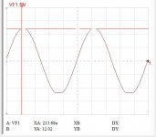
I find a good way to verify the distortion 'validity' in the sim is to plot FFT of input and output. If the input is not clean in the FFT, adjustments need to be done to the sim settings.
I don't understand why I get clipped at 12vp. 9w 1khz is 1%.
With your transistors the distortion is nearly the double.
Attachments

Last edited:
It's not obvious to me either. Your PSU is 27V, isn't it? If it were 24V it would clip at 12 for sure.
FWIW my simulation gives 0.29% at 9W and 10kHz using a 2N3019 and 0.23% with a BD139 driver, at 27V.
The driver almost cuts off in my sim with a standing current of 17mA, and going as low as 1mA. 10W shows the need for a higher voltage.
I have not simulated the 1969 design. The emitter current minimum for the driver transistor in the 1996 version using a constant current load is 10m.A. albeit this runs from +/- 22 Volt supplies for 15W into 8R.
In this setting the 2N3019 performed better than BD139 for THD. The former has a minimum fT of 100MHz with a maximum of 400MHz.
At 20k full power this gives room temperature THD of 0.15%. In operation the power transistors and the driver junctions will be far hotter, increasing loop gain for improved results.
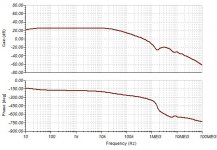
Room temperature Tian stability margin results for phase and gain were 45 degrees and 25dB.
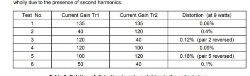
The distortion with mosfet driver passes from 0.08% to 0.017%. At 11w it is 0.05%.
With BC327/40 at the input it gives 0.015%.
Attachments
Last edited:
Those look useful developments.
My sims gave higher distortion for MJ15003. Not looked into that but strongly suspect a bad model, I'm wondering if that is the MODPEX one. Sounds like the 2N3055 model "out there" is not good either, which will not help designing with that device.
I'm sure there was a thread here somewhere which discussed models and their accuracy. But I hold manufacturers responsible primarily - it should not be up to others (like Andy C or Bob Cordell) to have to make better ones. However model verification is time consuming so I'm guessing some manufacturers aren't troubled too much to allocate resource even though that should lead to more sales, and happier customers, eventually.
just had a first run with an IRF610 driver. Got much higher distortion. Seems to be the gate current which is comparable to the input stage current. As with all designs there is a fair amount of work to do to check.
My old boss had a good view of this - "if a computer says something is not possible, it is probably right. If it says something is, check!"
Last edited:
You can respond in several ways. One response is to boycott the products from manufacturers whose SPICE models you don't like. Hit them where it hurts: in the pocketbook.
Another response is to call up your sales representative and demand a better SPICE model. Educate them why this should lead to more sales and happier customers, eventually.
Another response is to study the chapter in Bob Cordell's book and then extract the SPICE model parameters yourself. Now you are certain the model results are trustworthy: you've got plots of measured data on real devices, with the SPICE simulation results overlaid. They're as good a match as you are possibly able to make them.
Another response is to hire someone (for example, diyAudio member "keantoken") to measure the real device, create a SPICE model from those measurements, and then submit the results to you for final approval. If you approve, s/he gets paid 100% and you get the model parameter file. If you don't approve, s/he gets paid only 20% and you don't get the model parameter file.
- Home
- Amplifiers
- Solid State
- JLH 10 Watt class A amplifier