Can someone comment on the thermal stability of a quasi complementary output stage relative to the JLH output which can obviously be biased quite high? (With four NPN output devices on the heat sink along with the Vbe/bias device while the four drivers are mounted on the PCB without any heat sink)?.........
This kit/module is based closely on a successful and popular commercial product - Musical Fidelity's XA50. If there is a problem it is most likely with using over-the-top fast semis or trying to over-think the design requirements. The original power transistors and most others are craptanium types for low cost and TIP35C/36C are probably the most appropriate and original output types. The house numbers on the original parts were more likely used to silence adverse amateurish review comments about transistor quality.
However, LJM has commented elsewhere that that Lusya modules which use his PCB design, have problems but I didn't see any details. It would seem that it can only be component or semis problem. If that was your source, I'd compare pictures with all other versions if possible, including the small ceramic disc caps which look to me to have tempco issues. I have a couple of modules bought elsewhere, somewhere in my box of problems and they were unstable - haven't looked at them yet after seeing some little sqiggles and evidence of HF bursts on the 'scope.
Thank you for the reply.
As luck would have it I have two TIP35 and two TIP36 just arrived from Mouser. They were intended for a JLH but could be used elsewhere. (I was going to try one NPN and the other PNP/reverse all the polarities for fun.)
I have noticed that the MX50x2 output devices are not biasing evenly. So this evening I hunted down my IR thermometer (spot) and found that at idle with a pretty much cold heat sink the power transistor cases over the die are at significantly different temperatures. One is 40 degrees, two are 30 degrees and one is 24 degrees C. (Molding side over the silicon dies.)
Advice on next steps?
Tomorrow I might try triple checking the transistor to heat sink mounting.
If that results in nothing perhaps I try tossing out the kit supplied Silicon Rubber pads and use the few mica insulators that I have to see what happens.
If that results in nothing... ...perhaps I remove all the drivers and outputs and measure their hFE and Vbe???
Just think for a moment. The LJM design does work with DIO47/B817 output semis but probably of a specific brand that LJM uses or maybe specifies for his kits and modules. Unfortunately, you won't be able to uncover the important differences with a multimeter or generic semiconductor datasheets, as there are more parameters that govern transistor behaviour than you may care to know and I suspect the driver transistors could have a similar issue with different manufacturers too.
It's unlikely that you can remove the problems just by swapping output semis, now that the design has changed and component numbers are reduced. In any case, if you want to use original parts, don't forget to change them all and ensure that they are genuine parts, not another load of fakes, poor copies or "near enough" substitutes according to flaky opinions. Otherwise, you can't expect the problems to disappear unless you meet all the stability criteria of the original design. Believe me, that part is a design matter that isn't easy for anyone, let alone a beginner, to understand and formally investigate.
It's unlikely that you can remove the problems just by swapping output semis, now that the design has changed and component numbers are reduced. In any case, if you want to use original parts, don't forget to change them all and ensure that they are genuine parts, not another load of fakes, poor copies or "near enough" substitutes according to flaky opinions. Otherwise, you can't expect the problems to disappear unless you meet all the stability criteria of the original design. Believe me, that part is a design matter that isn't easy for anyone, let alone a beginner, to understand and formally investigate.
Last edited:
I don't really have anything solid to offer in the way of advice yet, other than to say that CFP output stages best derive their temperature reference for bias control from a transistor located right on or alongside one the drivers. The fact that this parallel CFP type clone has its temp. reference transistor located on the main heatsink with the output transistors, spells trouble or least inconsistency to me. For examples, take a look at ESP's P3A design or Douglas Self's Load Invariant amplifier design and chapters on CFP bias control in various handbooks, Self on Audio publications or modules offered at The Signal Transfer Company
I was wondering about that. I could take a piece of straight aluminum bar stock and drill five holes in it for the four drivers and then relocate the bias transistor from the main heatsink to this mini "heatsink".I don't really have anything solid to offer in the way of advice yet, other than to say that CFP output stages best derive their temperature reference for bias control from a transistor located right on or alongside one the drivers. The fact that this parallel CFP type clone has its temp. reference transistor located on the main heatsink with the output transistors, spells trouble or least inconsistency to me.
In the L20.5 and MX50SE, for example, there is a little heatsink on the PCB which contains the bias device and the drivers.
It would seem that it can only be component or semis problem. If that was your source, I'd compare pictures with all other versions if possible, including the small ceramic disc caps which look to me to have tempco issues. I have a couple of modules bought elsewhere, somewhere in my box of problems and they were unstable - haven't looked at them yet after seeing some little sqiggles and evidence of HF bursts on the 'scope.
What do you recommend instead of the high voltage blue ceramic 47 pF?
I don't have any "nice" caps that small. 1 nF is my smallest polyester film.
Do you know what dielectric is used in these 1 kV 47 pF blue caps? I don't see any mention from a few searches.
I could try to get some NPO/COG but I think vendor matters. Perhaps I can look for Murata or AVX 100V NPO/COG and solder them directly on the 649/669 or TTA004/TTC004 pins. (They are located collector to base so those are adjacent pins. So perhaps 100V quality NPO/COG SMD can solder right on the transistor.)
I am not sure I want to buy a much of silver mica capacitors for this project. Once I narrow down my favorite design I could justify more expensive components for that amp. But right now there are too many contenders: MA9S2 (current favorite), MX50x2, MX50SE, L20.5 and I still have the JLH to fire up after heatsinks arrive and some power supply work. And I almost forgot the L7 which is soldered together and awaiting test...
Well, having just seen this post, my first reaction is that the lower PNP driver transistor emitters should be fed through to the collectors of the lower NPN output transistors. That will put the quiescent current into a feedback loop, which is in the present circuit open ended.
I don't know if anyone said that - got to go and do something else, but will get back later.
I don't know if anyone said that - got to go and do something else, but will get back later.
Do you mean like I have drawn on the attached schematic?Well, having just seen this post, my first reaction is that the lower PNP driver transistor emitters should be fed through to the collectors of the lower NPN output transistors. That will put the quiescent current into a feedback loop, which is in the present circuit open ended.
Move the connection of both the 100 Ohm resistors and the 1N4007 diodes to the collectors of the lower NPN's?
Attachments
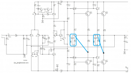
Yes, that's it.
Another point, I see the bias regulator is a pair of transistors. Are these a single packaged Darlington or two separate devices? Whichever, they both need to be mounted on the same heatsink as the output transistors. I presume they are?
And once there is some degree of NFB around the bias loop, the quiescent currents should be better matched, even if the transistors aren't.
If not then either there is a huge mismatch, or possibly the thermal resistance of the transistor mountings is not low enough.
The bias device is not a single packaged Darlington.Yes, that's it.
Another point, I see the bias regulator is a pair of transistors. Are these a single packaged Darlington or two separate devices? Whichever, they both need to be mounted on the same heatsink as the output transistors. I presume they are?
And once there is some degree of NFB around the bias loop, the quiescent currents should be better matched, even if the transistors aren't.
If not then either there is a huge mismatch, or possibly the thermal resistance of the transistor mountings is not low enough.
The smaller bias device is an NCC5551 on the PCB not attached to either the drivers or the heatsink.
The larger bias device is a 669 on the main heatsink along with the four K1047 output devices.
The drivers are two 649 and two 669 devices on the PCB and are not connected to each other or any heat sink. They are just four devices hanging in the air.
Photo attached. (Of the one that burned at +/- 50V). I am debugging the second board at +/- 25V but the bias is very uneven through the K1047 outputs.
Attachments
Hmm. I suspect the designer thought he could match the thermal heating of the drivers on the PCB with one device also on the PCB, and the output with the other on the heatsink.
I've found that the most stable arrangement is to have the drivers and output all on the same heatsink. Next best would have been to at least had a small aluminium plate on the PCB which the drivers and on-board thermal tracking transistor are connected. It's not a good idea to use free air and expect them to be thermally coupled.
Not sure how easy to mod this but possibly the drivers could be attached to a heatclip of some sort (even if the legs have to be extended with wires) and similiaryl find a way to attach the 5551 to the heatclip too. Even a small strip of aluminium might be enough.
Perhaps I can fit a small piece of aluminum bar stock along the fronts of the drivers and wedge it with the 5551 and spring type paper clips to test the idea.Not sure how easy to mod this but possibly the drivers could be attached to a heatclip of some sort (even if the legs have to be extended with wires) and similiaryl find a way to attach the 5551 to the heatclip too. Even a small strip of aluminium might be enough.
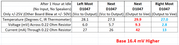
So one board burned up at +/- 50V (idle, in seconds) but I have made a few measurements on the surviving board. I have attached a table of my measurements that show that the lower D1047 transistors are not biasing up properly. You can see that the currents (and base voltage) are very different between the two D1047. This is at idle with no input and no speakers. This is after one hour at idle with very very low +/- 25V supplies
The bias through one D1047 is over 300% of the bias through the other D1047. 😱
What do you think is causing this problem? The base voltage is 16.4 mV higher on the D1047 with the much higher current.
Very large mismatch between the two 649 drivers? And/or outputs?
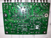
I was thinking my next step would be to pull the drivers and outputs and measure Vbe and hFE. At this point I would not be shocked to find that they are not matched at all at the factory. Soldering was quite messy. (See attached photo. Kind of looks like it was reworked or repaired?)
I suspect this is related to why the other MX50x2 burned up. By the way, the D1047 with the higher bias current gets much hotter than the other three when music is playing, even at pretty moderate volumes with only gentle +/- 25V supplies.
One last comment, the hot K1047/2SD1047 is dissipating only 0.042A * 25V = 1.05W. Yet the front of the transistor case/molding over the die area has risen 6 degrees C relative to the heatsink. That seems like a very poor thermal resistance doesn't it??? Best I can tell is that the metal tab of the transistor is close to the heatsink temperature so it looks like the majority of the thermal resistance is between the metal tab of the transistor and the silicon die.
Attachments
Last edited:
Well, it could be that you don't have matched transistors. But in the original circuit, again, there is nothing to ensure the currents in the two lower devices are properly shared. The resistors in the collectors in fact do nothing except add an IR drop and may as well not be there.
If you rearrange the circuit as discussed, this will address the problem. 1A through 0.22 ohms will generate enough of a voltage in one driver emitter to generate at least a nearly equal current in the other.
The other alternative would have been to add another pair of 0.22 ohm resistors in the emitters of the lower NPN's, but that means still needing a solution to ensuring that the current in the drivers is balanced i.e. still having to re-route the emitter resisotr/diode or adding extra resistors to ensure a current balance.
Once an unbalanced transistor gets hot, the Vbe falls below that of the other and that can lead to increased current.
This may be the problem you are seeing and the solution is the same as above.
I would also think that 0.22 ohm resistors is a little on the low side. I would normally select higher resistors, but that rather depends on the total load current expected.
If you are driving many amps into 4 ohms say, then 0.22 may be enough.
It might be worth checking too that the drivers are functional, and that the emitter resistors in the drivers, and diodes, are also working, because an open circuited driver connection might not be obvious immediately, but would mean one transistor not being driven properly.
And if the driver transistors have metal tabs on the back, remember to add mica washer or equivalent to insulate them from any metal strip.
Last edited:
Photo attached. (Of the one that burned at +/- 50V). I am debugging the second board at +/- 25V but the bias is very uneven through the K1047 outputs.
The frequency compensation scheme in this is over-complex. A simpler approach would have been to make C7 to be 100pF
This value is more common even seen in LJM circuits see-https://www.diyaudio.com/forums/solid-state/216609-ljm-mx50-kit-amp.html
Well, it could be that you don't have matched transistors.
I just pulled the drivers and they are very badly mismatched. 40 mV is quite a mismatch. Pictures attached.
1st measures Vbe = 641 mV and hFE = 153.
2nd measures Vbe = 601 mV and hFE = 148.
The mismatch in currents has improved but it looks like I need to pull, measure and replace the outputs too...
I replaced the drivers with ones that were matched in both Vbe and hFE as close as my meter reads after measuring every one I had.
But in the original circuit, again, there is nothing to ensure the currents in the two lower devices are properly shared. The resistors in the collectors in fact do nothing except add an IR drop and may as well not be there.
If you rearrange the circuit as discussed, this will address the problem. 1A through 0.22 ohms will generate enough of a voltage in one driver emitter to generate at least a nearly equal current in the other.
Yes. I have noted this. What I plan to do is pull/measure/match/replace the drivers and then the outputs. Then I will rearrange the circuit. That way I can quantify how much was caused by each issue.
It will take me a couple of days, assuming I have matched outputs to use.
Attachments
I would not use any other ceramic capacitor types for audio frequency purposes than NP0 dielectric.
As pretty as they may appear, those blue 1kV capacitors are made for voltage suppression - relatively a crude but effective dampening process.
As pretty as they may appear, those blue 1kV capacitors are made for voltage suppression - relatively a crude but effective dampening process.
"My original design is shown in Fig. 1. This is
still a valid design, except that the MJ4801481
output transistors are now obsolete. However,
they can be replaced by the more robust
2N3055. In this case, the epitaxial-base version of this device should be chosen rather
than the hometaxial, since the IT of the output
transistors should be 4MHz or higher.
As I commented, at the time, the design
gave a somewhat lower distortion if the hFE of
Trl was greater than that of Tr2' This caused
the output circuit to act as an amplifier with an
active collector load rather than an output
emitter follower with an active emitter load.
A simple modification which takes advantage of this effect is the use of a Darlington transistor such as an MJ3001 for Trl'
At I kHz, this reduces the distortion level at just
below the onset of clipping from about 0.1 %
down to nearer 0.01 %. As before, residual distortion is almost exclusively second harmonic.
Also, as before, it fades away into the general
noise background of the measurement system
as output power is reduced.
While this transistor substitution seems to be
a good thing, it was not a modification whose
effect I was able to check, in listening trials,
against the Williamson. As a result, for the
sake of historical fidelity, I would still recommend the use of epitaxial-base 3055s as Trl
and Tr2'
September 1996 ELECTRONICS WORLD
"Although directly coupling the amplifier to
the loudspeaker will not have much effect on
thd, it is still beneficial since it eliminates the
output coupling capacitor. The most obvious
way of doing this is to rearrange the input layout, around Tr4, so that it becomes the input
half of a 'long-tailed' pair.
I am reluctant to do this because this would
alter the overall gain/phase characteristics of
the amplifier. It would also require additional
high-frequency stabilisation circuitry, with all its incipient problems of transient intermodulation or slew-rate limiting." JLH
JLH was correct in his overview of converting the input stage to LTP. Using an LTP changes the nature of the design, and is often compensated by a Miller capacitor. Which as Old DIY reminds us, is the concern JLH had.
The designer has chosen to split the Miller capacitor into two, one small one (C7) and a larger one (C4) which is fed from the output rail. This is clearly an attempt to reduce distortion, but would be more appropriate for crossover distortion in a Class AB amplifier.
I assume this design operates in Class A.
In circuits JLH designed which used LTP input stage he usually chose to use inclusive compensation (RC series pair from collector of VAS to base of feedback side of LTP. Bailey used this successfully for a DC coupled amplifier, but that did not have a current mirror in the input stage, which adds more phase shifts and higher OLG. As probably pointed out in Bob Cordell's book, and earlier by Cherry, if the input stage LTP is degenerated the slew-induced distortion can be avoided. The loss of gain would need a Darlington VAS (emitter follower buffer if you separate the collectors I suppose).
Also the current mirror in this design ought to have small emitter resistors to balance the current a little better between the two devices.
This circuit seems to have overlooked a few things which have been learned in the last decade or two.
OK- just catching up with this. On another MX50 thread, it describes this as a 100W class AB design. This topic should probably not be in the JLH class A thread.
In which case, I would say that the input stage should be degen'd, the mirror pair have a small resistor (dropping a few tens of mV) to offset any Vbe mismatches, and the compensation capacitors should work, but whether tested properly I don't know. As mjona suggests, a single cap for C7 would be almost certainly guaranteed to work, but still needs degen input, I suggest, since the Re.C7 sets the upper frequency unity gain point.
The LTP current seems to be 0.6mA nominally. That is too small I think. Slew rate with 100pF is 6MV/s and most amps these days try to be 30MV/s or higher.
- Home
- Amplifiers
- Solid State
- JLH 10 Watt class A amplifier