Member
Joined 2009
Paid Member
looks very neat and compact - let us know how it sounds ! - watch the temperature of TR3 as it may get warm and a small piece of metal fixed to the transistor may be beneficial.
True double insulated should have no interaction at all
And have the following symbol on it (image from wikipedia)
An externally hosted image should be here but it was not working when we last tested it.
+1(in theory).
Making a dual polarity supply from 2 power supplies with floating output works well, I have just finish building a scaled down JLH 2005 (10W output) using 2 x 14Vdc power supplies. The AC mains is 2 prong and the supplies have the double square insulated symbol. Works like a charm and very good seller;
SMSL 1438T 14V3 8A Power Adapter for TA2020 TA2021 Amplifier LCD Laptop | eBay
BR,
Eric
SMSL 1438T 14V3 8A Power Adapter for TA2020 TA2021 Amplifier LCD Laptop | eBay
BR,
Eric
Both power supply are identical, same model no. same manufacturer. Each of these are rated up to 3.8A and I'm running them at 2.6A
This morning I have swapped both supply and the power supply that was running warm is still running warm (now feeding the - rail) so the issue is not the positive rail or Q2 drawing more current. 1 of the 2 power supply has an issue.
I have just order another one from e-pay to replace the warm one, I hope the new one will run cooler.
Thanks again to you all.
BR,
Eric
I bought another supply from the same epay seller and now both supply are running cooler 😛
Great sound, thanks to all.
Eric
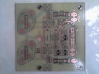
Can you share this pcb pdf?Just want to show off my layout for the JLH1969 😀
I haven't done any extensive tests yet, but it plays music so at least that's a good start. Board is 57*58mm and the output devices are MJL21196.
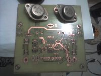
and on the bench for testing 😀
/U.
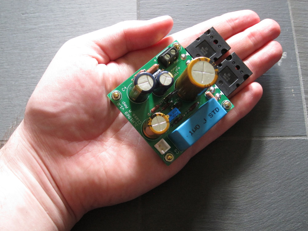
Think I forgot to post the PSU here.
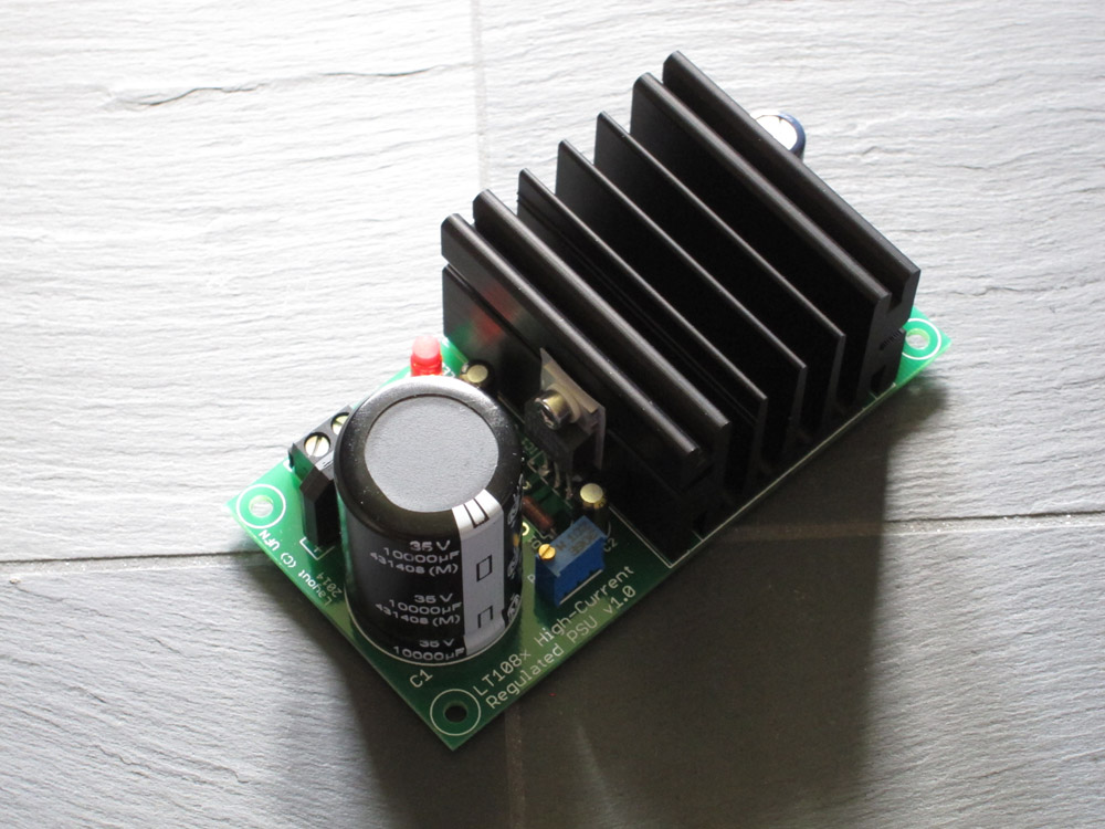
5x10 cm, using an LM1084 regulator and a Fischer SK68 heat sink which should be enough for one amplifier channel. The board works, there's a couple of small mechinical niggles, but nothing severe. Still haven't had time to test PSU and amp together, but hopefully this coming weekend will allow that 😀
/U.
Thermal coupling aids offset voltage control?
I have built a pair of the single rail version (on vero-pin-board as my homage to the original) and now want to build the 2005 version aiming for 35-40W and based on the SiliconRay board which seems to follow the “Final Circuit” (as shown on “The Class-A Amplifier site) exactly.
I like the idea of controlling the current through Q4 and Q5 as a way to manage the offset voltage as the amplifier warms up; especially as the mass of my heatsinks is going to result in a lengthy warm up period, and would appreciate some guidance.
Several knowledgeable posters in this long and rich thread have suggested that this works best if Q4 and Q5 are thermally coupled and the positioning of these two devices on the PCB would allow them to be kept in physical contact. At the extreme I assume I could use a through hole dual NPN device such as the 2N2920 (lots of $$) or slightly adapt an SMD such as a BC846BDW1T1G (a few cents) and have near perfect coupling. However, my knowledge is just enough to be dangerous and I am concerned that when using the result of differential heating to control the offset then surely thermal coupling would be exactly what was not wanted as it would prevent a temperature difference being created. I assume this is wrong as, presumably, it would apply to contact coupling as well.
No doubt I am missing something important here...
Member
Joined 2009
Paid Member
It should be perfectly adequate to have two separate TO-92 through-hole devices installed near each other with long enough leads so they can be slightly bent so that they are in physical (not electrical) contact with each other - ideally their two flat faces will touch. You can put some thermal grease in the contact area and hold them together with a bit of shrink-wrap, or you can glue them together with silicone glue (which remains flexible)
Specialized double-parts (through-hole) would be a waste of money in my opinion as there are likely other factors affecting the thermal stability of the offset that make this kind of matching silly. And don't bother with dual devices in SMD packages, I used them on my TGM5 against better advice and I would not use them again in a hurry (too darn fiddly).
Specialized double-parts (through-hole) would be a waste of money in my opinion as there are likely other factors affecting the thermal stability of the offset that make this kind of matching silly. And don't bother with dual devices in SMD packages, I used them on my TGM5 against better advice and I would not use them again in a hurry (too darn fiddly).
Last edited:
Think I forgot to post the PSU here.
5x10 cm, using an LM1084 regulator and a Fischer SK68 heat sink which should be enough for one amplifier channel. The board works, there's a couple of small mechinical niggles, but nothing severe. Still haven't had time to test PSU and amp together, but hopefully this coming weekend will allow that 😀
/U.
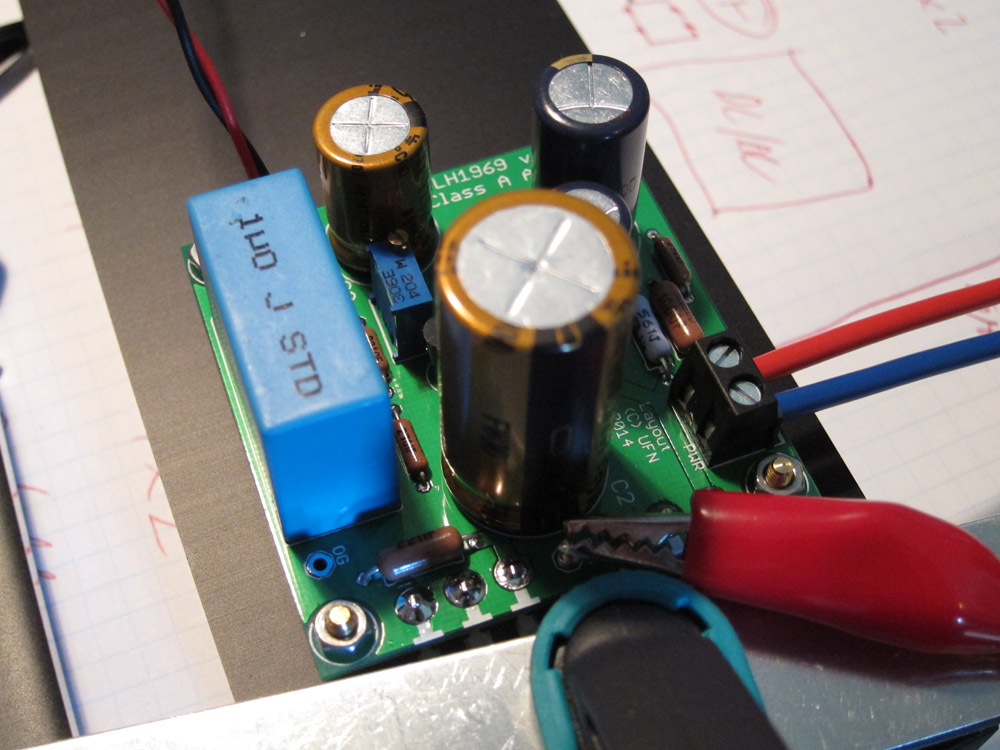
You could cut that heatsink in half as it's not going to be too effective with the regulator on one end of it.
Thank you Bigun - I seem to have put in more pre-ample than was helpful. I am happy with how to do this - but would like some help with the why i.e. this bit.
I am concerned that when using the result of differential heating to control the offset then surely thermal coupling would be exactly what was not wanted as it would prevent a temperature difference being created. I assume this is wrong as, presumably, it would apply to contact coupling as well.
Last edited:
Member
Joined 2009
Paid Member
Hi,
I don't know if I am going overboard with my response to your question, but here's the way I see it...
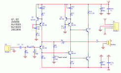
The dc-offset at the output is controlled by the global feedback loop in which Q4 is the active device with input at the base and feedback to the emitter. In terms of d.c. levels the current flowing through the collector of Q4 is mostly determined by the differential voltage across it's emitter-base junction. This collector current flows through a collector load resistor (R5) to create a voltage drop that provides a signal to the input of the VAS/phase splitter (Q3) and so on to the outputs, thus the current through Q4 controls the dc-offset at the output of the amplifier.
The control voltage for Q4 is the differential voltage between it's emitter and base. The voltage (with respect to ground) at the base of Q4 is some mV only, it is determined by the voltage drop developed across the base resistors (R2 and R3) by the base current flowing from Q4 base to ground. It's going to be small and stable so let's ignore it.
The dc voltage (with respect to ground) at the emitter of Q4 is going to be the dc-voltage at the output of the amplifier plus/minus any voltage drop across the series feedback resistor (R8) due to current flowing through that resistor, into the emitter of Q4. Because the emitter of Q4 must sit around 650mV more positive than the base (in order for Q4 to be conducting) it means that the output of the amplifier would have a dc-offset of at least 650mV plus the voltage drop across R8. This dc-offset would ensure that Q4 is biassed 'on' but it's not desirable for the speaker.
We can solve this problem if we provide the emitter of Q4 with an alternative supply of current and we do this by stringing up a constant current source (Q5 and Q6) from the +ve rail. This extra current 'pulls up' the voltage of the emitter of Q4 and allows Q4 to be biassed properly even when the dc level of the amplifier output is at ground. We adjust the current from the current source (VR3) until the amplifier settles to zero at the output.
The complication with this is that the current flow through Q4 doesn't simply depend on the differential control voltage across the emitter-base, it also has a temperature dependency. At higher temperature the current increases which moves the dc-offset at the amplifier output. What you have to do is reduce the current provided by the current source when the temperature increases, in order to allow the emitter voltage to drop back slightly and so keep the current through Q4 unchanged even when it warms up. And we can do that simply by allowing Q5 to warm up too, which causes Q5 to flow more current through it's collector load which in turn throttles back the output of the current source. The temperature dependency of Q4 and Q5 work together and balance out the affect of temperature changes. So you want Q4 and Q5 to be at the same temperature - by putting them in physical contact with each other. Voila.
I don't know if I am going overboard with my response to your question, but here's the way I see it...
The dc-offset at the output is controlled by the global feedback loop in which Q4 is the active device with input at the base and feedback to the emitter. In terms of d.c. levels the current flowing through the collector of Q4 is mostly determined by the differential voltage across it's emitter-base junction. This collector current flows through a collector load resistor (R5) to create a voltage drop that provides a signal to the input of the VAS/phase splitter (Q3) and so on to the outputs, thus the current through Q4 controls the dc-offset at the output of the amplifier.
The control voltage for Q4 is the differential voltage between it's emitter and base. The voltage (with respect to ground) at the base of Q4 is some mV only, it is determined by the voltage drop developed across the base resistors (R2 and R3) by the base current flowing from Q4 base to ground. It's going to be small and stable so let's ignore it.
The dc voltage (with respect to ground) at the emitter of Q4 is going to be the dc-voltage at the output of the amplifier plus/minus any voltage drop across the series feedback resistor (R8) due to current flowing through that resistor, into the emitter of Q4. Because the emitter of Q4 must sit around 650mV more positive than the base (in order for Q4 to be conducting) it means that the output of the amplifier would have a dc-offset of at least 650mV plus the voltage drop across R8. This dc-offset would ensure that Q4 is biassed 'on' but it's not desirable for the speaker.
We can solve this problem if we provide the emitter of Q4 with an alternative supply of current and we do this by stringing up a constant current source (Q5 and Q6) from the +ve rail. This extra current 'pulls up' the voltage of the emitter of Q4 and allows Q4 to be biassed properly even when the dc level of the amplifier output is at ground. We adjust the current from the current source (VR3) until the amplifier settles to zero at the output.
The complication with this is that the current flow through Q4 doesn't simply depend on the differential control voltage across the emitter-base, it also has a temperature dependency. At higher temperature the current increases which moves the dc-offset at the amplifier output. What you have to do is reduce the current provided by the current source when the temperature increases, in order to allow the emitter voltage to drop back slightly and so keep the current through Q4 unchanged even when it warms up. And we can do that simply by allowing Q5 to warm up too, which causes Q5 to flow more current through it's collector load which in turn throttles back the output of the current source. The temperature dependency of Q4 and Q5 work together and balance out the affect of temperature changes. So you want Q4 and Q5 to be at the same temperature - by putting them in physical contact with each other. Voila.
Attachments
Not overboard for me as you have moved me from ignorance to understanding so voila - I do indeed see... Thank you.
Thermal compound and heat shrink here I come!
Thermal compound and heat shrink here I come!
Looks good man, I like class A too! I'd be interested in seeing a frequency response if you get the chance.
Looks good man, I like class A too! I'd be interested in seeing a frequency response if you get the chance.
The the upper end goes into the 100s of kHz which probably counts as "more than enough" and the lower end is limited by the input capacitor 6db down at about 3Hz as shown. So, within reason, the frequency response is..... what you want it to be🙂
Member
Joined 2009
Paid Member
Extrapolating to the overall system, the lower end is limited by your room / speakers, the upper end is limited by your ears (if you're anywhere close to the average age of most hi-fi owners) so the response of the amplifier is mostly irrelevant 🙂
Member
Joined 2009
Paid Member
Well, I realize that I still haven't finished my dual-rail JLH69. I think I started it back in 2011, around post number 1882.
I looked at my notes on the topic. Seems the last time I played with this was last October (2014). Apparently I pulled out the carcass of the chassis I was making. I did get as far as building up a power supply on a pcbs of my own design. I tried it out with a resistive load on the power supply that resulted in a nearly 2A current draw. Ripple was around 600mV p-p. Unloaded, I was getting 26V per side (power trafo has two secondaries, one for each channel). Loaded, I was only getting 21V. This is a bit lower than I'd like to have. My notes also mentioned that I blew out the power supply fuse a few times on switch-on.
So, where next. Well, I'd like to finish something off, but I'm not going to invest much more into it. I think I'll parallel the power trafo secondaries to give me more current driver and build a mono-block into the chassis I have. I have a soft-start circuit lying around unused I can use to tame the switch-on demands too.
Last edited:
- Home
- Amplifiers
- Solid State
- JLH 10 Watt class A amplifier