The 0.87v across Q4 B-E suggests either a problem or that a fairly large base current is flowing.
Is there any voltage across R5 ? Normally there should be around 1.3 volts across here.
If there is no voltage across R5 then remove Q3 (or at least isolate the base lead) and recheck the voltage across R5. Has it come up ?
Is there any voltage across R5 ? Normally there should be around 1.3 volts across here.
If there is no voltage across R5 then remove Q3 (or at least isolate the base lead) and recheck the voltage across R5. Has it come up ?
The 0.87v across Q4 B-E suggests either a problem or that a fairly large base current is flowing.
Is there any voltage across R5 ? Normally there should be around 1.3 volts across here.
If there is no voltage across R5 then remove Q3 (or at least isolate the base lead) and recheck the voltage across R5. Has it come up ?
For my measurement, I have an 8 ohm load and the input is shorted.
There is no voltage across R5 before and after isolating (cutting) the base of Q3.
You mentionned 1.3V across R5 which is a 8k2, this mean a current of 0.15mA...seems a little too low should I increase the value of R5..I wish I could simulate this circuit to see what value I should use for R2, R5 and R9.
R2 (base of Q4) is 15K but the majority of schematic I have seen uses 47k, can this cause the high Vbe ?
Thanks a lot.
Eric
Last edited:
For testing don't have any load connected. Its to risky both for the load and the output transistors.
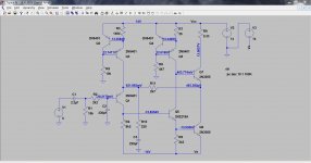
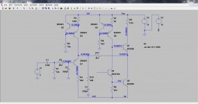
Yes, in normal operation there will be around 1.3 volts across R5. That's a non varying value and determined by the two B-E volts drops of Q3 and Q1 added together.
You can simulate it 🙂 Here is the file that will run straight off in LTSpice. No extra models needed.
These two images show the normal voltages and the voltages when Q3 base was open.
The component refs in the sim are different to your picture
Attachments
This is awesome, thanks a lot for the simulation.
My load is simply a 25W, 8 ohm resistor.
If I remove the load I get +14Vdc on the output...
BR,
Eric
My load is simply a 25W, 8 ohm resistor.
If I remove the load I get +14Vdc on the output...
BR,
Eric
Thanks a lot for your help Mooly, the amp is now working and warming up the place !
I had to replace Q4, Q7 and Q8 from my schematic.
BR,
Eric
I had to replace Q4, Q7 and Q8 from my schematic.
BR,
Eric
Thanks a lot for your help Mooly, the amp is now working and warming up the place !
I had to replace Q4, Q7 and Q8 from my schematic.
BR,
Eric
Excellent 🙂 Well done.
Help please.
Well, you guessed it I'm back with some more issues with the second channel 😀
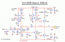
I have attached the schematics with the DC voltage shown in red, these are referenced to gnd.
Q1, Q3 both have Vbe of 0V even though I just changed them.
Q7 is kinda odd with a Vbe of about 0.18 and it varies based on the value of VR2.
You want to laugh ? Have a look at the Vb of Q4, a whopping 6.4V...while input is tied to gnd. To top it off a nice 21V across R5 🙂
If you have any idea what's happening please share your knowledge.
Thanks a lot,
Eric
Well, you guessed it I'm back with some more issues with the second channel 😀
I have attached the schematics with the DC voltage shown in red, these are referenced to gnd.
Q1, Q3 both have Vbe of 0V even though I just changed them.
Q7 is kinda odd with a Vbe of about 0.18 and it varies based on the value of VR2.
You want to laugh ? Have a look at the Vb of Q4, a whopping 6.4V...while input is tied to gnd. To top it off a nice 21V across R5 🙂
If you have any idea what's happening please share your knowledge.
Thanks a lot,
Eric
Attachments
Last edited:
Question 2
What is hfe of Q5 Q6 - are they BC560 a, b or c - I remember someone saying that to high hfe here can cause problems.
What is hfe of Q5 Q6 - are they BC560 a, b or c - I remember someone saying that to high hfe here can cause problems.
At face value Q3 is open circuit. 21 volts across B-E. That is what the voltages show on the diagram. You say you have checked/replaced Q3. Open circuit print to the base of Q3 ?
Ah yes, I see now. With Q3 open there is no current across R9. That explains the-14V on the base of Q1.
BOTH channels fixed !
Hi,
Well Mooly was right on once again. The problem was Q3..transistor was fine but the PCB trace between Q3 base and Q4 collector was broken therefore open circuit 😀 By looking at it the trace and solders looked fine.
Both channel now have nearly zero DC offset and are biasing nicely and stable at 1.3A/ch.
Thanks a million guys !
BR,
Eric
Member
Joined 2009
Paid Member
I don't have a proper set-up yet since the amp is in the garage, been listening through an iPod and a pair of BR CSS EL70.
I will soon report back but from what I heard it's promising.
Thanks all.
Eric
I will soon report back but from what I heard it's promising.
Thanks all.
Eric
Great to hear you have it up and running. Enjoy 🙂
Hi,
It's working OK but I have the following potential issue I'd like to fix.
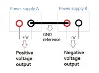
I'm using 2 power supply (switching) each rated with a single 14V, 3.8A output. These PS each have floating output so with 2 of them I'm able to create the required +/-14Vdc, 3.8A for my stereo set-up.
One of the SMPS (laptop type, brick style) is heating up uncomfortably while the second one is only warm.
Is there a way to share the load equally between my 2 power supply so 1 of them doesn't stop working prematurely ?
If that doesn't work, where can I buy a +/- 15Vdc, 120-150W power supply.
Thanks,
Eric
- Home
- Amplifiers
- Solid State
- JLH 10 Watt class A amplifier