Hello,
Shielding or guarding sensitive things is often a good idea.
Human brain, even my cat; a strange unusual sound will jump to our attention.
Can we measure TIM?
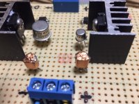
The image appears not to have posted.
Thanks DT
Shielding or guarding sensitive things is often a good idea.
Human brain, even my cat; a strange unusual sound will jump to our attention.
Can we measure TIM?
The image appears not to have posted.
Thanks DT
>Can we measure TIM?
It is difficult to measure TIM directly, but phase margin change in frequency may corresponds TIM.
Lesser phase margin change is low latency index of amplifier.
It is difficult to measure TIM directly, but phase margin change in frequency may corresponds TIM.
Lesser phase margin change is low latency index of amplifier.
Attachments
Last edited:
Bottom line we do not want our line level preamplifiers, crossover followers and the like adding any perceptible noise.
Are you building microphone amplifiers??
If not, then your hiss level is already set by your source material and its microphone amplifier. (Or unfortunate audio processing.) (Or vinyl surface noise.)
Or do you mean: the hiss when there is NO signal?
There is topic of related TIM here. (Written in Japanese)
オーディオのイシノラボどっとこむ - 店長のブログ >>店長のブログ>> ブログアーカイブ >> NFBアンプを考えてみよう!
Google translate
Google Translate
He is former engineer of SANSUI.
He said,
In the listening, Important thing is "audible or not audible" for us.
The noise masks very small signals, but other nonlinear factars also masks very small signals.
"the input signal are not correctly calculated due to the phase delay" means **dynamically generated noise like signal for us** may masks very small signals.
But it is difficult to measure by sine wave.
Then you have to evaluate your own ears.
For example, "My favareite" OPA659 (GBW 650MHz, SR 2550 V/μs, ±6V max) has excelent spatial ambience (depth feeling, hall ambience, breathing, etc).
In other words, it makes very small signals still audible.
They has flat open loop phase responses in audible frequency.
In the JFET, I like 2SK168.
It also has nice spatial ambience.
オーディオのイシノラボどっとこむ - 店長のブログ >>店長のブログ>> ブログアーカイブ >> NFBアンプを考えてみよう!
Google translate
Google Translate
He is former engineer of SANSUI.
He said,
I think,NFB theoretically knows that if there is no time delay, there is no negative effect of NFB, but the problem is how much phase delay (time delay) is at which frequency. In Sansui, the frequency characteristics before applying NFB (open loop characteristics: or naked characteristics) are set to at least the audible band, and NFB is designed to be applied over a wide range without time delay.
At higher frequencies, NFB's adverse effects were minimized by the 2-pole phase compensation theory technique that reduces the amount of NFB by reducing the phase delay as much as possible.
The negative effects of NFB are the phenomenon that the feedback signal and the input signal are not correctly calculated due to the phase delay and cannot be detected by the continuous signal, but the so-called transient characteristic deteriorates. In the 1970s, Matti Otara predicted that I think that the thing called (transient intermodulation) also refers to this.
In this way, I think that the Sansui amplifier has mastered the NFB.
Therefore, even if the distortion rate is measured with a continuous signal and the same measurement result is shown, there is no doubt that this is the reason that there are amplifiers with different sound quality. How to hang NFB is important.
In the listening, Important thing is "audible or not audible" for us.
The noise masks very small signals, but other nonlinear factars also masks very small signals.
"the input signal are not correctly calculated due to the phase delay" means **dynamically generated noise like signal for us** may masks very small signals.
But it is difficult to measure by sine wave.
Then you have to evaluate your own ears.
For example, "My favareite" OPA659 (GBW 650MHz, SR 2550 V/μs, ±6V max) has excelent spatial ambience (depth feeling, hall ambience, breathing, etc).
In other words, it makes very small signals still audible.
They has flat open loop phase responses in audible frequency.
In the JFET, I like 2SK168.
It also has nice spatial ambience.
Attachments

Last edited:
BOTHAre you building microphone amplifiers??
If not, then your hiss level is already set by your source material and its microphone amplifier. (Or unfortunate audio processing.) (Or vinyl surface noise.)
Or do you mean: the hiss when there is NO signal?
Hello PRR and All,
I agree completely that the SOURCE in terms of noise can and will dominate everything else.
For fun and information see this old Fairchild AN6605.
https://www.onsemi.com/pub/Collateral/AN-6605.pdf.pdf
At this point I am not building anything. The focus is to dig a little deeper into JFET Parameter measurement, maybe even matching, including noise. Things like 1/f, thermal noise and corner frequency. The intrinsic noise of a JFET may be well below that of the source. However, I still want to take a closer look.
For fun and information see this old Siliconix AN106.
https://www.vishay.com/docs/70599/70599.pdf
I am still puzzled over this question. Should the JFET noise be measured in a DUT configuration where all the other sources of noise can be factored out with only the JFET noise remaining? Or a more practical real world DUT test circuit that includes all the resistors and the like that will be part of a working circuit?
Once all this is sorted, all the source noise and JFET circuit noise theoretically can be calculated and or measured.
For fun and information see this Marshall Leach assignment.
https://leachlegacy.ece.gatech.edu/ece6416/Labs/exp05.pdf
Thanks DT
Hiss? My least favorite is hum and buzz where there should be silence.
I built and heared his NchJFET buffer and tested some JFETs.
2SK168: Internally cascaded VHF band JFET (Source and Drain are incompatible). It has wide depth feeling and excellent spatial ambience. It brews reality.
2SK772: wide depth feeling and good spatial ambience. but 2SK168 is better than this.
2SK336(2SK170): Tolerably depth feeling. In spite of their NF, I feel cloudy than 2SK168 and 2SK772.
2SK117: 2SK336 is slightly better than this.
J112: slightly better than 2SK336?.
"Spatial ambience" is very small level and it may be located in relatively higher frequencies because bats are using ultrasonics for their echolocation.
Those signals may be susceptible by latency of amplifier in their shorter periodic cycles.
Then high speed 2SK168 has excellent spatial ambience.

Why not include the 2SK30 as well? It is certainly capable of generating a generous spatial ambience. (I modestly call it high frequency response).
A transistor's ability to respond to weak signals is inversely related to its ability to respond to high frequency signals.
A transistor's ability to respond to weak signals is inversely related to its ability to respond to high frequency signals.
2SK30 is may be better than 2SK170.
I not have 2 pair of 2SK30.
I think that this problem is not frequency response.
Could you compensate it by equalizer?
2SK170 has adequate higher frequencies, but spatial clearity is cloudy than 2SK168.
In spite of contents includes spatial informations, but 2SK170 is degrades it.
2SK168 makes it still audible.
The reason behind the excellence of 2SK30 is low gain. It affects all aspects of performance but predominantly at high frequencies. You cannot circumvent this intrinsic property.
2SK170 exhibits much higher gain therefore higher distortion, popular because it has a complementary pair.
Is the 2SK30 still obtainable in Japan? It is at the top of my list anyway.
2SK170 exhibits much higher gain therefore higher distortion, popular because it has a complementary pair.
Is the 2SK30 still obtainable in Japan? It is at the top of my list anyway.
2SK30 is used by Mr. Kaneta who is famous amplifier designer.
2SK30 has smaller capacitance which may reduce latency which is related to TIM.
2SK168 Ciss 6.8pF, Crss 0.1pF
2SK30 Ciss 8.2pF, Crss 2.6pF
2SK170 Ciss 30pF, Crss 6.0pF
2SK772 Ciss 9.0pF, Crss 2.1pF
2SK208 is SMD version of 2SK30.
2SK30 has smaller capacitance which may reduce latency which is related to TIM.
2SK168 Ciss 6.8pF, Crss 0.1pF
2SK30 Ciss 8.2pF, Crss 2.6pF
2SK170 Ciss 30pF, Crss 6.0pF
2SK772 Ciss 9.0pF, Crss 2.1pF
2SK208 is SMD version of 2SK30.
Last edited:
Note that both Ciss and Crss change as a function of VDS, or VDG.
IOW, not only the choice of semiconductor, but the choice of operating voltages can be used as an additional tool for adjusting the performance, stability and sonic parameters of a given circuit.
Note that VDS will affect gate leakage currents (more noticeable for N-JFETS than P), and will also impact the noise level, both of which are likely to impose a practical limit on how much the VDS can be increased.
hth
Hello,
I not have model of 2SK168.
2SK168 is lager gate leakage current (10nA max), but it can be competitive for bipolar audio op-amps.

2SK30ATM Ciss 8.2pF, Crss 2.6pF
2SK30 is one of best seller JFET, someone may wants SMD version.
I not have model of 2SK168.
Attached image is Crss vs Vds curve of 2SK168.Note that both Ciss and Crss change as a function of VDS, or VDG.
2SK168 is lager gate leakage current (10nA max), but it can be competitive for bipolar audio op-amps.
2SK208 Ciss 8.2pF, Crss 2.6pFI don`t trust the 2SK208. Ciss is not that relevant, Crss is.
2SK30ATM Ciss 8.2pF, Crss 2.6pF
2SK30 is one of best seller JFET, someone may wants SMD version.
Last edited:
Kaneda san popularized the 2SK30. I don`t trust the 2SK208. Ciss is not that relevant, Crss is.
Each person is welcome to make their own experiments and draw their own conclusions, but my own testing suggests that Ciss can be very relevant indeed.
Show us your test methods and results.
This thread is less about conclusions, more about tests and results.
Show us your test methods and results.
Thanks DT
Each person is welcome to make their own experiments and draw their own conclusions, but my own testing suggests that Ciss can be very relevant indeed.
This thread is less about conclusions, more about tests and results.
Show us your test methods and results.
Thanks DT
I replied to the discussion starting with
JFET’s J113, 2SK170, 2N5457 and others
where audible effects of various JFET choices were raised.
My testing involved building dozens of otherwise-identical test circuits where a single parameter such as semiconductor choice or VDS was altered, then scoping the circuit (for stability, noise and offset), then listening blind.
Last edited:
Ciss is associated with current gain and Crss is associated with voltage gain. The 2SK30 has a very high channel resistance giving small signal amplitudes and low distortion, and is in practice unusable as a voltage amplifier. A high operating voltage is a bad idea.
Latency is a nonsensical term in this context and there is no reason to worry about TIM.
Latency is a nonsensical term in this context and there is no reason to worry about TIM.
End of Life PF5102 JFET at Mouser.com
🙂Hello All,
I am back to visit a bit.
Last chance to buy the PF5102 JFET. Mouser.com has just two more deliveries coming in December of 2019
The PF5102 is a Process 51 N channel JFET, the J113 and J111 are brothers differing only by IDSS.
The PF5102 on the data sheet is 4mA min to 20mA.
I just received a last chance End of Life package for 10 Cents each.
Thanks DT
I will post test results of typical IDSS and curves a little later.
- Home
- Amplifiers
- Solid State
- JFET’s J113, 2SK170, 2N5457 and others