The layout follows exactly Greg's final, the stable version - with one exception:
I have changed the Zener used for the input biasing to two LEDs in series.
It can compete with Hugh's design, when it comes to size and price.
It measures only 95 x 75mm in size and costs about 11€ per PCB (Quantity = 10 PCBs).
swordfishy Greg's final stable circuit which is the model for your PCB.
But we replace zener with 2 red LED-diodes
I show the circuit here. Regards Rudi 🙂
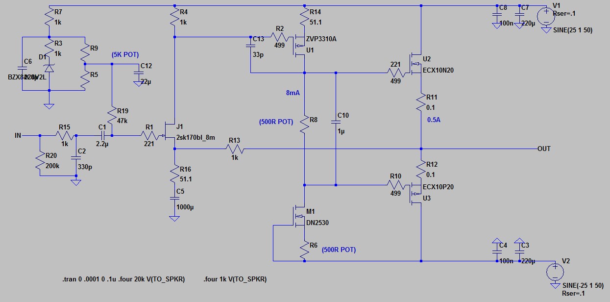
That is the source for my layout, Lineup! 😉
And I replaced D1 by two red LEDs.
Best regards - Rudi_Ratlos
P.S. I see, that I have to replace R8 by a trim potentiometer?! Will be no problem!
And I replaced D1 by two red LEDs.
Best regards - Rudi_Ratlos
P.S. I see, that I have to replace R8 by a trim potentiometer?! Will be no problem!
Last edited:
@Lineup,
just to show you, how quickly components can be changed, if you own a powerful layout software:
http://www.abload.de/img/topviewoi6x.png
Best regards - Rudi_Ratlos
P.S. I will rename this layout to "Greg's original FETZILLA".
just to show you, how quickly components can be changed, if you own a powerful layout software:

http://www.abload.de/img/topviewoi6x.png
Best regards - Rudi_Ratlos
P.S. I will rename this layout to "Greg's original FETZILLA".
Last edited:
I have MultiSim with UltiBoard. Think it is powerful.
But I use only sim and do no boards.
But it looks as fun to do 🙂
"Greg's Original FETZILLA"
is a good name to refer to.
And it is a solid version. I just simmed it.
It shows good performance and low distortion.
But I use only sim and do no boards.
But it looks as fun to do 🙂
"Greg's Original FETZILLA"
is a good name to refer to.
And it is a solid version. I just simmed it.
It shows good performance and low distortion.
one question about the AC coupled version:
Does the electrolytic cap in the feedback path maintain an offset bias at all times, max i/p signal etc ?
probably obvious to some but I haven't thought about it till now
Does the electrolytic cap in the feedback path maintain an offset bias at all times, max i/p signal etc ?
probably obvious to some but I haven't thought about it till now
The voltage across the cap should stay practically the same.
It will be an average of voltage at JFET Source - Ground 0Volt
But if we should fead positive pulses the voltage should increase across cap.
It will be an average of voltage at JFET Source - Ground 0Volt
But if we should fead positive pulses the voltage should increase across cap.
I have always thought about the cap
as being normal polarized electrolytic cap.
I think it should be overdoing it to use a non-polar or bipolar.
No need but if anyone bothers to use non-polar so ...
Normal quality e.g. 1000uF electrolytic is my standard.
as being normal polarized electrolytic cap.
I think it should be overdoing it to use a non-polar or bipolar.
No need but if anyone bothers to use non-polar so ...
Normal quality e.g. 1000uF electrolytic is my standard.
I suggest using DN2540.
The benefit over DN2530 is more headroom for max power out.
In short, using DN2540 gives at least an extra Watt out.
The difference is not big.
But the drop across source resistor of
DN2530 at 8 mA is
0.008mA x 253.7 Ohm = 2.03 Volt
And DN2540 at 8 mA
0.008mA x 174.5 Ohm = 1.40 Volt
Compare this to red LED CCS ~1.10 Volt
Max out at THD 0.100%
with DN2530 23.66 Watt
with DN2540 24.89 Watt
with LED CCS >25 WAtt
Using one red LED current source
we can pass the Magical level 25 Watt
Using two transistors CCS we can sqeeze the most out.
Hi Rudi ,
Are interested in the 6 PCB.
Regards,
Vitali
Are interested in the 6 PCB.
Regards,
Vitali
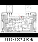
... and this is yet another layout of the Fetzilla - in its pre-final layout status.
I call it: "Poor People's Fetzilla". 😛

http://www.abload.de/img/topviewxcbr.png
It can in no technical way compete with Hugh's high-sophisticated design - for sure.
The layout follows exactly Greg's final, the stable version - with one exception:
I have changed the Zener used for the input biasing to two LEDs in series.
It can compete with Hugh's design, when it comes to size and price.
It measures only 95 x 75mm in size and costs about 11€ per PCB (Quantity = 10 PCBs).
My German DIY-friends would like and have a group-buy for this PCB (they would even have it "as a kit: PCB + 5 transistors").
If there is some interest in this forum as well, I will ask a DIY-friend to organize this group-buy.
Please tell me: are you interested in the "PP Fetzilla"?
Best regards - Rudi_Ratlos
P.S. The quality of the PCB will be the very best, that you can imagine: 2mm thick PCBs, 70µm copper traces, gold-immersion, silkscreen ...

well using ohms law if we have 7mA i/p bias current and it all flows through a 1K FB resistor and if the o/p is at zero then we have 7V across the cap - that sounds ok to me.
Interestingly when I tried to check this in simulation, my first AC coupled simulation effort, it oscillated violently and nothing I could do would make it stop - I never once had this with the DC linked one - I wonder why this would be
Interestingly when I tried to check this in simulation, my first AC coupled simulation effort, it oscillated violently and nothing I could do would make it stop - I never once had this with the DC linked one - I wonder why this would be
... and this is yet another layout of the Fetzilla - in its pre-final layout status.
I call it: "Poor People's Fetzilla". 😛
http://www.abload.de/img/topviewxcbr.png
It can in no technical way compete with Hugh's high-sophisticated design - for sure.
The layout follows exactly Greg's final, the stable version - with one exception:
I have changed the Zener used for the input biasing to two LEDs in series.
Best regards - Rudi_Ratlos
Hi Rudi,
Well done, nice layout.
I have build one of the Swordfishy's versions which uses two LEDs to bias the JFET. I noticed a potential error with your PCB: the connection of the wiper of the 5K trimpot. In other word, R9+R5 together make up the 5K trimpot.
C6 is a 220uF, so it should be a electrolytic capacitor, it shows a film cap in your layout.
One more suggestion:
Make space for a three-LED string. I tried to run a higher bias current thru the K170 but I ran out of bias voltage because I use two LEDs.
Cheers, Stanley
Attachments
Last edited:
Yes 3 LEDs for the input bias is better.
Feedback cap always has a positive voltage across it. Non polarized is fine. I use good quality panasonic fc caps. Work quite well.
Depletion mode MOSFET ccs is better for many reasons. I posted many of these a page or two back in the thread. The only negative is that it is not as perfect as a current source when compared to a bjt ccs. However it is more than adequate for the intended purpose and has many advantages such as very low noise and low latch up.
It is far closer to being a perfect current source than a real life bootstrap, and just as simple. Very good sonically too.
Last edited:
What is missing in Rudi's PCB is Zobel.
It could be put across the output terminals.
But it is better to have that possibility on the board.
Out - 10 Ohm - 47nF - GND
It could be put across the output terminals.
But it is better to have that possibility on the board.
Out - 10 Ohm - 47nF - GND
Actually in Greg's final Fetzilla the current is ~2.75mAwell using ohms law if we have 7mA i/p bias current and it all flows through a 1K FB resistor and if the o/p is at zero then we have 7V across the cap - that sounds ok to me.
which makes 2.75Volt across the cap.
This way 2 red LED can be used to create 2.75V.
(The drop across 2 LED is like 3.3 or 3.4 Volt)
Actually I think it was more like 3.5 - 4mA. If not, the drain resistor should be lowered to keep the current at 4-5mA. It will depend on the Vgs of your vas fet.
Yes, it depends on the actual value of VGS in the MOSFET.
For IRF9610 we can count on ~3.8 Volt VGS
In that case we better use 3 LEDs.
My simulation with your final schematic (Drain resistor 1k) shows 2.76mA
Drain resistor 560 Ohm gives 4.92mA
Drain resistor 680 Ohm gives 4.05mA
Drain resistor 820 Ohm gives 3.36mA
Drain resistor 1k Ohm gives 2.76mA
This is with the ZVP3310 model in spice
Did you notice it sounded any better with filters in ?
Hi Mikelm,
I did a back-to-back test, the volume is slightly softer with the filter in. The sound is definitely better with the filters "IN" whilst playing violin concerto.
My tests was real easy, I used an pair of crocodile(alligator) leads to short out the two resistors. I did that whilst the amp was powered on.
Try that on your setup & tell us the finding.
I may have to drop the R from 33ohm to 22ohm.
The voltage drop across the positive rail R is 0.8V,
The voltage drop across the negative rail R is 0.37V
Cheers, Stanley
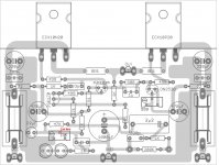
I made the changes to my layout and inserted a Zobel:

http://www.abload.de/img/topview17po.png
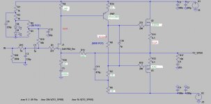
This is the schematics of my layout:

http://www.abload.de/img/schematicso75p.png
I am looking forward to your improvements - if any.
Best regards - rudi_Ratlos

http://www.abload.de/img/topview17po.png
This is the schematics of my layout:

http://www.abload.de/img/schematicso75p.png
I am looking forward to your improvements - if any.
Best regards - rudi_Ratlos
- Status
- Not open for further replies.
- Home
- Amplifiers
- Solid State
- JFET input, MOSFET VAS, LATERAL output = Perfect!!