Simple SWF BJT version
Hi all,
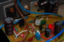
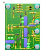
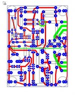
I finally got one Fetzilla version going. I used an old PCB as a base, cut a few traces & few more holes & many jumpers - so the PCB layout is less than optimal.
I build the Greg's simple BJT version - just 4 active devices & no compensation capacitor. The sound is pretty good for such a simple circuit, it lack a little bit of bass but vocal is the one that shines. My build has a low-level hum (I have 16400uF main filter for each rail) & I have not added the RC filter for the front end. The output offset voltage drifts a bit.
I am using a 2SA1538 as VAS & I will add a MOSFET CCS to compare.
The only small N-MOSFET that I got is 2SK3840 & I will try that first.
Is there any specific reason to use the Depletion mode DN2530 for the CCS role?
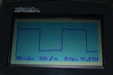
The square wave is 13.7kHz.
Cheers, Stanley
Hi all,
I finally got one Fetzilla version going. I used an old PCB as a base, cut a few traces & few more holes & many jumpers - so the PCB layout is less than optimal.
I build the Greg's simple BJT version - just 4 active devices & no compensation capacitor. The sound is pretty good for such a simple circuit, it lack a little bit of bass but vocal is the one that shines. My build has a low-level hum (I have 16400uF main filter for each rail) & I have not added the RC filter for the front end. The output offset voltage drifts a bit.
I am using a 2SA1538 as VAS & I will add a MOSFET CCS to compare.
The only small N-MOSFET that I got is 2SK3840 & I will try that first.
Is there any specific reason to use the Depletion mode DN2530 for the CCS role?
The square wave is 13.7kHz.
Cheers, Stanley
Attachments
Hi Stan,
Nice work! Well done for actually building something and listening.
Your observation that the vocals shine is spot on.
You may have noticed in my earlier comments that the bootstrap vas really does not perform as well in the bass department, though the vocals are surreal. If you want better bass you will need to build a vas with a ccs. It is a huge improvement. This is verified not only by listening tests but also in simulation.
Also, a fet sounds much nicer in the vas, and has better bass, but I understand you are working with what you have.
As for the ccs, the depletion fet offers a few advantages but is not mandatory. I have made a very nice sounding ccs using an irf610 n channel fet and two LEDs. The advantages of the depletion mode device are:
Ultimate simplicity and reliability.
Practically impossible to have oscillation problems (with the ccs itself).
Pretty much latch up proof.
No other active devices (zeners, etc) to induce noise into the circuit.
As a second best go with an n channel fet or npn transistor and an LED voltage reference. I think if you search this thread for irf610 you will find an example that I have posted. It sounded very good.
Last edited:
Hugh,
Please feel free to go ahead and post the schematic used on the pcb, including all capacitors, diodes, zeners, etc. The purpose of some of these might not be immediately apparent so a brief circuit description might be useful....if you are willing and have the time.
Please feel free to go ahead and post the schematic used on the pcb, including all capacitors, diodes, zeners, etc. The purpose of some of these might not be immediately apparent so a brief circuit description might be useful....if you are willing and have the time.
Oh, all, one thing I may not have mentioned previously.
I never knew where I stood on the subject of break in for amplifiers. I was not sure whether there was anything to the concept or whether it was all a load of hogwash. However, I am convinced that a few hours of running really improves things for this amplifier. If you build it you may notice a smoother, more fluid and relaxed presentation begin to develop after a few hours of continuous operation. I'd be interested to know if anyone else notices the same thing or whether it's all in my head.
I never knew where I stood on the subject of break in for amplifiers. I was not sure whether there was anything to the concept or whether it was all a load of hogwash. However, I am convinced that a few hours of running really improves things for this amplifier. If you build it you may notice a smoother, more fluid and relaxed presentation begin to develop after a few hours of continuous operation. I'd be interested to know if anyone else notices the same thing or whether it's all in my head.
It's not in your head, Greg. It's a function of caps and semis bedding in and it's well known, documented widely, but pooh poohed by many. It is definitely noticeable.
Hugh
Hugh
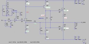
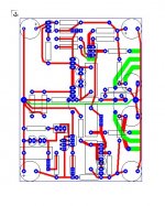
Here is the PCB I am planning to make for my next DC linked prototype with a DC drift cancelling element and provision for a Hawksford cascode both of which are as yet untested ( but either could be left unused )
I don't regard my self as very expert at PCB layout so all comments / suggestions are welcome.
I don't know how to place components on the track side with my PCB program so certain places look a bit crazy but the o/p snubber and psu filter resistors will be on the track side.
I don't regard my self as very expert at PCB layout so all comments / suggestions are welcome.
I don't know how to place components on the track side with my PCB program so certain places look a bit crazy but the o/p snubber and psu filter resistors will be on the track side.
Attachments
Last edited:
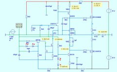
Here is the diagram that roughly corresponds to this board, the hawksford cascode is not shown here but can easily be spotted on the pcb.
My main filter caps are off board.
The lower CCS is designed to have equal & opposite DC drift characteristics to the VAS / i/p element. I'm reasonably sure that it will reduce DC drift quite a lot but I have to assess for any impact on the sound.
On the board there is provision for dual zvn3310 or 4424 VAS devices. The i/p filter cap will be underneath also
Attachments
Last edited:
Only reason is the simplicity. Takes only one resistor to make a CCS.Is there any specific reason to use the Depletion mode DN2530 for the CCS role?
Just like with JFET.
Makes very high PSRR.
What we use plays no big role. Most any CCS will do.
Agree with Lineup, Mike, well done.
Still wrestling with the schematic, want to incorporate the lot.....
Hugh
Still wrestling with the schematic, want to incorporate the lot.....
Hugh
Mikelm, you may want to look at Hugh's board for some circuit ideas.
my head starts to spin when I look at Hugh's board 😉
HughStill wrestling with the schematic, want to incorporate the lot.....
Hugh
It is not easy. With Fetzilla.
I have said there is almost as many versions as builders.
Or even more versions.
Incorporate a couple of options and so.
Maybe this makes it reasonable. Less impossible.
RC filter for the front-end rails
I added 33R+1000uF RC filter to both front-end power rails, now the low-level hum is gone. The RC filter is very effective.
My build has a low-level hum (I have 16400uF main filter for each rail) & I have not added the RC filter for the front end.
I added 33R+1000uF RC filter to both front-end power rails, now the low-level hum is gone. The RC filter is very effective.
I added 33R+1000uF RC filter to both front-end power rails, now the low-level hum is gone. The RC filter is very effective.
Did you notice it sounded any better with filters in ?
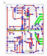
I think I've now got a version of the board that covers almost every version of this amp that I can remember.
I made it easier for myself because certain things like diodes, filter caps, input caps ( yes, it also does the AC linked version ) are all off board - and I put some components on the bottom of the board
I'm not getting into competition with Hugh, I don't really want to get into the hassle of shipping boards all over the globe, but if one or two people, preferably in UK or Europe would like to share the costs of making these boards that would be great.
I only just finished last element so I will take a couple more days to check everything and would appreciate any input to check for mistakes etc.
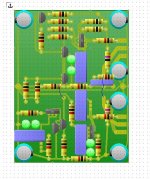
I show here the boards set up for the AC linked version
some components bottom left are redundant in this version
I made it easier for myself because certain things like diodes, filter caps, input caps ( yes, it also does the AC linked version ) are all off board - and I put some components on the bottom of the board
I'm not getting into competition with Hugh, I don't really want to get into the hassle of shipping boards all over the globe, but if one or two people, preferably in UK or Europe would like to share the costs of making these boards that would be great.
I only just finished last element so I will take a couple more days to check everything and would appreciate any input to check for mistakes etc.
I show here the boards set up for the AC linked version
some components bottom left are redundant in this version
Attachments

Last edited:
p.s.
I did not include a boot strap as such, but with all the pads there it would be easy to improvise one.
o/p mosfets need a 90 degree aluminium bracket for mounting.
I did not include a boot strap as such, but with all the pads there it would be easy to improvise one.
o/p mosfets need a 90 degree aluminium bracket for mounting.
... and this is yet another layout of the Fetzilla - in its pre-final layout status.
I call it: "Poor People's Fetzilla". 😛

http://www.abload.de/img/topviewxcbr.png
It can in no technical way compete with Hugh's high-sophisticated design - for sure.
The layout follows exactly Greg's final, the stable version - with one exception:
I have changed the Zener used for the input biasing to two LEDs in series.
It can compete with Hugh's design, when it comes to size and price.
It measures only 95 x 75mm in size and costs about 11€ per PCB (Quantity = 10 PCBs).
My German DIY-friends would like and have a group-buy for this PCB (they would even have it "as a kit: PCB + 5 transistors").
If there is some interest in this forum as well, I will ask a DIY-friend to organize this group-buy.
Please tell me: are you interested in the "PP Fetzilla"?
Best regards - Rudi_Ratlos
P.S. The quality of the PCB will be the very best, that you can imagine: 2mm thick PCBs, 70µm copper traces, gold-immersion, silkscreen ...
Last edited:
- Status
- Not open for further replies.
- Home
- Amplifiers
- Solid State
- JFET input, MOSFET VAS, LATERAL output = Perfect!!