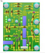
I also have been tweaking my board design and now I think I have all the elements I need to try all the versions of this amp that I am interested in.
I tried to ensure that the large o/p current paths were in equal & opposite directions so that the electromagnet fields would not interact with other stages of the amp - so I am quite happy with this part.
I'm not so sure about how I did the earthing - but I've made a a lot of amps like this and I didn't experience any problem.
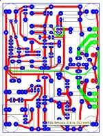
On my board i/p cap, rectifier diodes & main PSU filter caps are off board and some components are on the solder side.
This is an ideal board for anyone curious to experiement with many different versions but particularly DC linking.
This is the feature set for this board:
AC Coupling with caps biased.
DC Coupling with non servo offset control.
Lead and / or lag compensation.
Pads for either irf9610 or BD140 or ZVP3310 etc VAS .
Possibility for 2 x zvp3310 or 4424 as VAS.
Bootstrapped or CCS VAS.
Pads for hawksford cascode.
o/p snubber.
R C filters both legs.
Extra RC filters for AC coupled biasing or DC offset control.
multiple pads for different sized caps.
Features not included:
DC servo
Cascoded VAS
I can get these boards for about £10 each and less if I'm patient about delivery
I have the feeling DC linking isn't a hot topic for many here but if anyone is interested - let me know.
mike
I tried to ensure that the large o/p current paths were in equal & opposite directions so that the electromagnet fields would not interact with other stages of the amp - so I am quite happy with this part.
I'm not so sure about how I did the earthing - but I've made a a lot of amps like this and I didn't experience any problem.
On my board i/p cap, rectifier diodes & main PSU filter caps are off board and some components are on the solder side.
This is an ideal board for anyone curious to experiement with many different versions but particularly DC linking.
This is the feature set for this board:
AC Coupling with caps biased.
DC Coupling with non servo offset control.
Lead and / or lag compensation.
Pads for either irf9610 or BD140 or ZVP3310 etc VAS .
Possibility for 2 x zvp3310 or 4424 as VAS.
Bootstrapped or CCS VAS.
Pads for hawksford cascode.
o/p snubber.
R C filters both legs.
Extra RC filters for AC coupled biasing or DC offset control.
multiple pads for different sized caps.
Features not included:
DC servo
Cascoded VAS
I can get these boards for about £10 each and less if I'm patient about delivery
I have the feeling DC linking isn't a hot topic for many here but if anyone is interested - let me know.
mike
Attachments
Last edited:
Stanley,
Nice, thanks for the work. Got any more comments about the sound? I'm eagerly awaiting your thoughts on the addition of a ccs to the vas. I think it will cure your bass woes...
Hi Greg,
I have not listened to the simple-BJT bootstrap version for long enough to give a good assessment.
As it is, the amp sounds very good with a bit of low frequency roll-off. It is not the most detailed amp that I own but the sound is rich & musical. It sounds like a tube amplifier; may be it has a good dose of 2nd harmonics.
I don't want to dismantle this version, I will build another channel with IRF9610 as VAS & IRF610 as CCS so that I can compare. I have a couple of those old PCBs laying around.
Have to good trip.
Cheers, Stanley
Mike,
Paul and I spent the day in discussion of this circuit.
Along the lines you allude to above, we concluded that because of a very large switch on thump, it would be better to eschew the shunt fb cap, simply ground the 47R shunt fb resistor, replace the input jfet with a mosfet like the DN2530, and servo it. This should enhance the bass response too. I use this approach in one of my designs, it is absolutely foolproof and sounds very, very good.
This is the direction I will head with the pcb layout, which can be set up for off board power supply as well.
There will be some additional complexity, but I believe the glitch free operation makes this the best way to progress the design.
Cheers,
Hugh
any of the equivalent Lateral mosFETs will do.Where can you buy the ECX10N20A-10P20A?
did already find that website😀
and this one http://www.peats.com/cgi-bin/catalog_v2.cgi?type=product&id=2527
Are these usefull http://www.class-d.com/lateral-mosfets/cat_14.html
and this one http://www.peats.com/cgi-bin/catalog_v2.cgi?type=product&id=2527
Are these usefull http://www.class-d.com/lateral-mosfets/cat_14.html
Last edited:
Wouldn't be better to reduce the gatestoppers by a factor 10 and move the generated phaseshift a decade up
I just checked this in spice ( still no square wave gen in the real world ) and I found that sq wave ringing - with 100nF at o/p - is indeed much reduced when gate stoppers values are reduced.
I began with 270R and saw initial 10V peak to peak ringing lasting for 15uS
reducing to 47R gave 7V P2P lasting for about 6uS
reducing to 20R gave only marginal improvement perhaps about 5uS
reducing to 10R showed no discernible difference at all.
So if you have short leads to your o/p mosfets, then I agree with Sonnya that reducing gate stopper is a valuable method of increasing stability and perhaps will give the amp even more sparkle 🙂
I would try 47R first and see how it looks on the scope with square waves.
Thanks Sonnya - I saw this in simulation years ago but had forgotten about it.
mike
Last edited:

Way to go.
I would not remove them at all as amp design tends to have long traces (more than 10mm) and therefore you will get seriesinductance playing with Ciss,Crss.
- Sonny
http://www.microsemi.com/micnotes/APT0402.pdf
While beads might kill local parasitic oscillation, I'm not sure
what it does to closed loop stability? Adding an inductance
seems counterproductive when inductance IS the problem.
But perhaps lossy resistance at high frequency is greater?
One of those things that never sims well for me, but might
be just the ticket IRL...
Last edited:
I think lowering the gate stoppers decreases Miller action at the VAS because of the reduced drive voltage necessary to charge the gates. This decreases the effective compensation of the amp. A simple conclusion is that the decreased compensation decreased the output inductance of the amp, decreasing Q and ringing. However this may be simplistic unless the amp has very well-behaved output impedance phase (which is quite possible for this amp).
- keantoken
- keantoken
Thanks, Ken! From that article:
APT0402.pdf said:It has been found that a ferrite bead combined
with a resistor on each MOSFET gate
eliminates
parasitic
oscillation
while
minimizing switching losses. In fact, adding a
ferrite bead is more effective than using gate
resistance alone because the impedance of the
ferrite bead is directly proportional to
frequency. The bandwidth of the gate drive
signal is about 2MHz, whereas parasitic
oscillation frequency is many times higher,
from about 50MHz to 250MHz. So the
impedance of the ferrite bead to oscillation
noise is 25 to 125 times higher than its
impedance to the gate drive signal. This high
impedance is extremely effective at blocking
drain to gate noise current. Given enough
inductance in the ferrite bead combined with
sufficient damping from the gate resistance,
parasitic oscillation can be completely and
reliably eliminated.
o/p degeneration resistors.
I noticed that nearly everyone including me has been using 0.1R o/p resistors but a few have questioned their necessity so I did some research in spice and my conclusion was that they didn't add anything to the design and the amp is probably better without them.
I took mine out and I think it sounded better but the amp is still running in and sounding better each day anyway.
I guess it's convenient to have a 0.1 resistor to measure o/p bias current but I think they would be better placed up stream somewhere rather than in the signal path.
Just in case I left the wrong impression before I just wanted assure people that this is a very nice sounding amp indeed.
mike
I do not use such OP-Source resistors in my SPICE of Fetzilla.
My philosophy is to remove everything possible.
As long a resistor is not shown to do any real improvement. And is needed.
Laterals seem do not need.
But IRFXXX and bipolar need them.
mike
Good to hear your amplifier is good working and sounding already.
My philosophy is to remove everything possible.
As long a resistor is not shown to do any real improvement. And is needed.
Laterals seem do not need.
But IRFXXX and bipolar need them.
mike
Good to hear your amplifier is good working and sounding already.
normally the source resistors are used for current sharing purposes in multiple output arrays.
They are not needed on laterals due to their negative tempco...not even if multiple pairs are used...
I always put them in for simulation,, as the are a convenient tool to monitor currents in the Op-stage
They are not needed on laterals due to their negative tempco...not even if multiple pairs are used...
I always put them in for simulation,, as the are a convenient tool to monitor currents in the Op-stage
Member
Joined 2009
Paid Member
I like the JFET input version, definitely looks interesting, glad I 'found' this thread.
However, I'm thinking JFET = TRIODE and a nice hybrid maybe what's in my future.
However, I'm thinking JFET = TRIODE and a nice hybrid maybe what's in my future.
Bigun. Welcome.
It is an enormous thread!
Sometimes like looking for a needle in a haystack.
But all guys here are friendly and willing to discuss
different versions of The Fetzilla amplifier with JFET input stage
and Laterals output stage.
It is an enormous thread!
Sometimes like looking for a needle in a haystack.
But all guys here are friendly and willing to discuss
different versions of The Fetzilla amplifier with JFET input stage
and Laterals output stage.
Thanks, Ken! From that article:
Interesting paper.
Any suggestion for a ferrite bead part number (axial lead) from a big supplier (Mouser. digikey, etc...) to use with these Lateral Mosfet?
Interesting paper.
Any suggestion for a ferrite bead part number (axial lead) from a big supplier (Mouser. digikey, etc...) to use with these Lateral Mosfet?
Wurth elektronik is a good supplier. They produce high quality ferrites, beads, inductors and so on.
A ferrite bead impedance curve is a bit like an inverted capacitor impedance curve. You have a peak in the impedance at a specific frequence. Above this parasitic capacitance start to be dominant.
You have to go through the datasheets. If there is no impedance curve - skip them.
Or go for Murata and TDK.
I think these 3 is the easiest to get you hands on. But the nost of them is SMT ... Sorry
I think these 3 is the easiest to get you hands on. But the nost of them is SMT ... Sorry
- Status
- Not open for further replies.
- Home
- Amplifiers
- Solid State
- JFET input, MOSFET VAS, LATERAL output = Perfect!!