Well, now your clippling on the negative input/positive output cycle  But you've reconfigured the circuit.
I think there was a question originally. It is now becoming 2 or more different questions (all other things being the same )
My guess(not knowing all the other parameters) is: In the first shot, you are overdriving the input, or loading the output to much, for the designed current, voltage and gain. There could be room for improvement in that respect with some slight changes. In the second shot, you should be experimenting with the B1 not JBOZ. I don't see any benifit in reducing the JBOZ to a unity gain design.
😉
But you've reconfigured the circuit. I think there was a question originally. It is now becoming 2 or more different questions (all other things being the same
)My guess(not knowing all the other parameters) is: In the first shot, you are overdriving the input, or loading the output to much, for the designed current, voltage and gain. There could be room for improvement in that respect with some slight changes. In the second shot, you should be experimenting with the B1 not JBOZ. I don't see any benifit in reducing the JBOZ to a unity gain design.
😉
I am not necessarily interested in unity gain.
I am just trying to illustrate that no matter what I do to this circuit it will not accept greater than 500mV (amplitude) at the gate of the jfet without some sought of clipping.
While Tschrama version does not have this problem.
What is happening here?
Can it be fixed?
If I needed 8V rms (11.2V peak amplitude) I would rather use the full 2Vrms from the cd player to get my 8Vrms (gain of 4).
But with this circuit so far I can only manage for it to accept 500mV (peak amplitude) so to get my 8V rms (11.2V peak amplitude) I need a gain of about 22.
This will still work, but then the circuit will need a better power supply, because your working with a smaller signal at the input.
If this can't be fixed I will just accept the fact, and build it anyway, but I would really like to fix this problem.
thanh1973 said:
If I needed 8V rms (11.2V peak amplitude) I would rather use the full 2Vrms from the cd player to get my 8Vrms (gain of 4).
But with this circuit so far I can only manage for it to accept 500mV (peak amplitude) so to get my 8V rms (11.2V peak amplitude) I need a gain of about 22.
This will still work, but then the circuit will need a better power supply, because your working with a smaller signal at the input.
If this can't be fixed I will just accept the fact, and build it anyway, but I would really like to fix this problem.
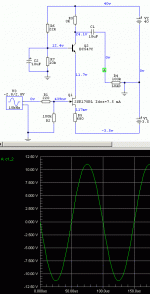
I think what you are seeing is this simple circuit is not appropriate for an output of 8 V rms (22.4V pk-pk)
To get that kind of *clean* output, you probably need a circuit working from rails of maybe 2X the pk-pk voltage. Most common would be say +/- 24 V rails.
thanh1973 said:...If I needed 8V rms (11.2V peak amplitude)....
Here you are (2Vrms IN - 8V rms OUT):
Attachments
Sorry BFNY you missed my point.
The point has nothing to do with output voltage. It has to do with the fact this circuit will not accept greater 500mV at the input.
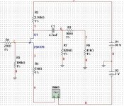
Here is another image. On the left is the original version with slight resistor changes to reduce the gain slightly. On the right is the Tschrama version.
The point has nothing to do with output voltage. It has to do with the fact this circuit will not accept greater 500mV at the input.
Here is another image. On the left is the original version with slight resistor changes to reduce the gain slightly. On the right is the Tschrama version.
Attachments
thanh1973 said:Just for confirmation the 439nV at the gate is DC right.
Yes
thanh it might have something to do with the fact that original JBOZ does not have feedback.
What happens when you put your probes at the other side of R4, directly at the gate?
What happens when you put your probes at the other side of R4, directly at the gate?
I just checked that.
I get the same result for original version, however with Tschrama version signal has dropped when measure right at the gate.
I have got a long way to go before I fully understand all there is to know about this hobby (probably never).
I get the same result for original version, however with Tschrama version signal has dropped when measure right at the gate.
I have got a long way to go before I fully understand all there is to know about this hobby (probably never).
The version on the left is the topology (without particular values) I was refering to. BOZ, open loop etc. and will be subject to the 1/2V or so, clipping your seeing. Whenever the Gate is approximately 1/2V below(negative) the Source, you will be approaching Vpinch(No current flow) and it will be in clipping.
However, anyone can help me out here...
The version on the right however has feedback This will basically cause a 0V summing node at the Gate.
  When the feedback loop is satisfied, something less than 1/2 the V1 input voltage (due to the 12.6k voltage divider R1 & R2) is all across your 11k input resister. The output voltage, now an opposite polarity, will be all across your 22k feedback resistor. Therefore there is no voltage at the Gate node. It is unlikely you can swing the source node positive enough with signal to cause -1/2V G-S. The circuit can still clip, but not from the gate to source overload the open loop design encounters. 😀
However, anyone can help me out here...
The version on the right however has feedback
This will basically cause a 0V summing node at the Gate. When the feedback loop is satisfied, something less than 1/2 the V1 input voltage (due to the 12.6k voltage divider R1 & R2) is all across your 11k input resister. The output voltage, now an opposite polarity, will be all across your 22k feedback resistor. Therefore there is no voltage at the Gate node. It is unlikely you can swing the source node positive enough with signal to cause -1/2V G-S. The circuit can still clip, but not from the gate to source overload the open loop design encounters. 😀thanh1973 said:Sorry BFNY you missed my point.
The point has nothing to do with output voltage. It has to do with the fact this circuit will not accept greater 500mV at the input.
You were right all along, and it was a great observation. The question is why. It was answered in the Borbely article on JFETS, the link is here
http://www.borbelyaudio.com/adobe/ae599bor.pdf
the author states (top of pg 4 left column) -
"The most obvious difference between
the two JFETs is in the maximum input
swing with which you can drive them.
The K170 allows approximately ±0.1V
peak before the gate goes positive, but
the K246 has a range of ±0.5V! Naturally,
I could move the working point further
down on the transconductance curve in
order to increase the input range, but
eventually I would reach the other limiting
point, where the gate cuts off at VP.
The thing to understand here is that a
high-VP JFET has a wider range of input
swing than one with a low VP."
You already have the explanation why the other circuit with feedback to the gate accepts larger input voltages (but the gate voltage is reduced by the feedback)
So to deal with large input gate voltages, you need to select another JFET that has a higher value of Vp. A good choice is the J310, but there are many others.
Bob
It doesn't matter if Gate goes positive in absolute sense, it is important that it doesn't go positive in respect to Source.
If Gate measures +2v and source is on +3V everything is still OK because even in that case Gate is on -1V potential in respect to Source.
That's what Rs (Source resistor) is for. Source potential varies with Id and that's what determines (together with Rd - Drain resistor and gm-transconductance) the gain of this simple circuit.
juma said:It doesn't matter if Gate goes positive in absolute sense, it is important that it doesn't go positive in respect to Source.
If Gate measures +2v and source is on +3V everything is still OK because even in that case Gate is on -1V potential in respect to Source.
That's what Rs (Source resistor) is for. Source potential varies with Id and that's what determines (together with Rd - Drain resistor and gm-transconductance) the gain of this simple circuit.
Good to point that out, the difference between the "bias point", which is a DC setting, the "no input signal" static Vgs (voltage, gate minus source) and then the input signal AC voltage swing around that bias point. The input signal voltage swing can be expressed in terms in static +/- DC voltage levels, which equal peak to peak AC levels, or AC rms levels.
As with tubes, if you have a low impedance source, you can drive the Vgs slightly positive. But for linear operation best to stay in the negative Vgs area.
Hi,
previous post:
so original NP Pre circuit has gain of only 0.06? sorry I don't know
enough to understand this.
can I use this pre circuit for gain of +10dB? if so, which resistors values should I change? I'll be using the +16V PSU.
my goal is to boost pre-out level of my AVR into an external amp that has 47K input impedance. All I know is the AVR is suppose
to be capable of 1.25Vrms on the line out.
thanks.
previous post:
-24dB corresponds to roughly a gain of 0.06 and not simply an inversion of the 16x gain. Normally you would characterize the system with both gain measured in dB and phase and then this phase would characterize any inversion of the signal.
so original NP Pre circuit has gain of only 0.06? sorry I don't know
enough to understand this.
can I use this pre circuit for gain of +10dB? if so, which resistors values should I change? I'll be using the +16V PSU.
my goal is to boost pre-out level of my AVR into an external amp that has 47K input impedance. All I know is the AVR is suppose
to be capable of 1.25Vrms on the line out.
thanks.
Bengali said:Hi,
previous post:
so original NP Pre circuit has gain of only 0.06? sorry I don't know
enough to understand this.
can I use this pre circuit for gain of +10dB? if so, which resistors values should I change? I'll be using the +16V PSU.
my goal is to boost pre-out level of my AVR into an external amp that has 47K input impedance. All I know is the AVR is suppose
to be capable of 1.25Vrms on the line out.
thanks.
The post is refering to a previous misunderstanding of the dB scale. Don't worry, the jboz has plenty of gain. 😀
14dB version
I changed the value from Juma's original circuit.
2.94K and +30V. with the sim, I get about 14dB gain.
for my needs, max Vin is 1.25Vrms. I get 6.22Vrms out.
how bad would the distortion be? is this pushing it too far?
I don't know how to check for distortion,etc.. with the sim.
just know the barebones stuff with the demo.
thanks
Attachments
- Home
- Amplifiers
- Pass Labs
- Jfet BOZ