Self oscillating ones?
We have to note the difference between controller and driver here.
Typically the controllers, while they look perfect for the job, are not meant to handle the kind of voltages audio requires, they usually lack in some respect.
I think you're right on about the disable pin. Also some drivers only have 1 input, others have 2. This is one difference between the ir2111 and ir2101. I would design the circuit fo the IR2101, for it has much less internal dead time, and you can gain full control over both inputs, it is a recommended part for audio.
Did you look at the app notes of IR?
there is an interseting and simple design for a 200w+200w with the IR 2011, wich looks a lot at what i want to achieve.
On the top of your head, do you have others suggestions of more commonly available power mosfets?
the IRFB23N15D seems to be used a lot in D amps, but feature a 0,1 ohm RDS on, wich i found high compared to others with 0,0xxx ohms rds on.
thanks.
Simple ? 
I can't recommend any MOSFETS off hand..
I'd keep looking for a simpler design, with feedback taken after the filter for best performance. I admire your ambition!
I can't recommend any MOSFETS off hand..
I'd keep looking for a simpler design, with feedback taken after the filter for best performance. I admire your ambition!
I Have Parts for your amp
Dear Pat,
I have parts and modules for your specific amp. According to the picture your amp has been repaired without original parts. I have original parts for your amp. Approximate cost is 80 dollars CAD. If you are interested PM me for contact information I am based in Toronto, Ontario.
Dear Pat,
I have parts and modules for your specific amp. According to the picture your amp has been repaired without original parts. I have original parts for your amp. Approximate cost is 80 dollars CAD. If you are interested PM me for contact information I am based in Toronto, Ontario.
Re: I Have Parts for your amp
You're really goign to sell him a part which is based on a defective design for 80$?? C'mon man, a UCD 180 is 100 Euro and it isn't defective. Give it away or throw it out
cantech said:Dear Pat,
I have parts and modules for your specific amp. According to the picture your amp has been repaired without original parts. I have original parts for your amp. Approximate cost is 80 dollars CAD. If you are interested PM me for contact information I am based in Toronto, Ontario.
You're really goign to sell him a part which is based on a defective design for 80$?? C'mon man, a UCD 180 is 100 Euro and it isn't defective. Give it away or throw it out
Thanks, i already answered him. I have ordered all the parts to build a IRAUDAMP a la International Rectifier, i got all the components to build 4 modules (1 chanel each) for around 50$ CDN...i have build my own PCB (1ch) for testing, i will build a better one with 2 channels for a bridged mode and throw a lot of watts, wich will be cool for my TL project for my home.
Thanks.
Thanks.
classd4sure said:Hi Zach,
I think I can take a pretty good guess why...
Look at the circuit! Total build cost (mass produced).. I'm not sure.. less than a dollar???
The PSU caps exploding.... because they pinched more pennies and sized them too small.. Obviously, quality is not a concern for them. Just think, someone probably got a big fat check for recommending this topology with respect to every penny they pinched.
Kept you busy though, didn't it? I only hope this screw up cost them far more than it made them! I noticed your key words "that they keep putting out" ...
Unfortunately, JBL never offered a fix for this problem. I actually spent more time on the phone getting replacement subs for customers than I did actually fixing the dead ones. JBL (and Infininty) ended up offering customers accomadation pricing for replacement subs that were still under warranty instead of fixing the problems that they had. And, I'm sure that this SNAFU ended up costing Harman International quite a bit of money over the course of this whole mess.
pat allen said:
Hi Zach, since you are a JBL service center (still?), you might have some good connection with the company?
What i am looking for is the original schematic of the S64AMI module, because i cant figure some components values in mine.
If you cant, do you have someone that i can reach and ask.
Thanks.
BTW, i melted everything.
It never worked as it should, the best i did get is with a lot of tweaks, and it was not that much good.😡
Here is a link to the PB12 service manual:
PB12 Service Manual
It doesn't look like there is a schematic for the module, but there are schematics for the rest of the amp.
Cheers,
Zach
classd4sure said:Hi Zach,
Look at the circuit! Total build cost (mass produced).. I'm not sure.. less than a dollar???
so cheap? what kind of gate driver did they use?
the schematic on the user's manual is too small and I can't recognize the words on the chip.
Kenshin said:
so cheap? what kind of gate driver did they use?
the schematic on the user's manual is too small and I can't recognize the words on the chip.
Gate driver? In my opinion, they didn't have one. The user manual doesn't show the modulator at all, see this post:
http://www.diyaudio.com/forums/showthread.php?postid=543572#post543572
Pat Allen:
my god, s64ami just used some 7414 paralleled to drive MOSFET gate! It's a fault design even for (robot race) motor drivers. And it's a part of a commercial audio D-amp design?!
perhaps BJT P+N emitter follower will be more powerful(but it needs design again)
At least,replace them using an 555,this can operate safely at 12V.
These are more than repairing. let's go to thread "Output devices" to talk.
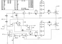
S64AMI schematic and parts list
Hopfully Pat will be viewing this, as it pertains specifically about his reverse engineered S64AMI schematic. I found several flaws in it, errors in the circuit paths, and most notibly the parts values you listed are way off. If anyone has tried to breadboard this thing by that schematic, I would bet they didn't have much luck!
If I can figure out how to attach an image, I will put the corrected parts values and the schematic on here for everyone. I don't have that program that allows me to write PDF's, so Pat, If you wish to re-write this so it is in a better format, PLEASE DO!
What I did is take a screenshot of the PDF and altered it using a paint program so at least I had something. Sorry about the large JPG fellas! I didn't want to loose what little detail was left!
S64AMI schematic and parts list
Hopfully Pat will be viewing this, as it pertains specifically about his reverse engineered S64AMI schematic. I found several flaws in it, errors in the circuit paths, and most notibly the parts values you listed are way off. If anyone has tried to breadboard this thing by that schematic, I would bet they didn't have much luck!
If I can figure out how to attach an image, I will put the corrected parts values and the schematic on here for everyone. I don't have that program that allows me to write PDF's, so Pat, If you wish to re-write this so it is in a better format, PLEASE DO!
What I did is take a screenshot of the PDF and altered it using a paint program so at least I had something. Sorry about the large JPG fellas! I didn't want to loose what little detail was left!
I do have actual scans of both sides of the raw circuit board, so if anyone is interested in them, let me know and I will post them too.
Jeremy
Attachments
Hi Jeremy,
At the bottom when you're writing a post where it say's "attach file".... simple. Try saving your file as a PNG, no loss of quality, even in MSPaint, and very small size.
Can always zip it further if you have to.
Looking forward to seeing your corrections.
Take care.
At the bottom when you're writing a post where it say's "attach file".... simple. Try saving your file as a PNG, no loss of quality, even in MSPaint, and very small size.
Can always zip it further if you have to.
Looking forward to seeing your corrections.
Take care.
Re: S64AMI schematic and parts list
Hi i would like to see the original schematic for sure. BTW, i never said my reverse was perfect, and that i was unable to deliver correct parts values because they are unreadable. But at some point, i did make it work on my bread board, until some parts fryed because of a stupid mistake.
I didnt worked any further on it since i have done something quite better, and is under work for now.
Post anything you have about this module.
Thanks.
charger_1 said:Hopfully Pat will be viewing this, as it pertains specifically about his reverse engineered S64AMI schematic. I found several flaws in it, errors in the circuit paths, and most notibly the parts values you listed are way off. If anyone has tried to breadboard this thing by that schematic, I would bet they didn't have much luck!
If I can figure out how to attach an image, I will put the corrected parts values and the schematic on here for everyone. I don't have that program that allows me to write PDF's, so Pat, If you wish to re-write this so it is in a better format, PLEASE DO!
What I did is take a screenshot of the PDF and altered it using a paint program so at least I had something. Sorry about the large JPG fellas! I didn't want to loose what little detail was left!
Hi i would like to see the original schematic for sure. BTW, i never said my reverse was perfect, and that i was unable to deliver correct parts values because they are unreadable. But at some point, i did make it work on my bread board, until some parts fryed because of a stupid mistake.
I didnt worked any further on it since i have done something quite better, and is under work for now.
Post anything you have about this module.
Thanks.
uploaded wrong schematic!
OOPS! Not only did I upload the wrong schematic, I did it twice! (had troubles earlier)
Hopfully I got the right one this time.
The differences are that D8 and D9 are not zener diodes, and d7 is supposed to be 1n4937.
Sorry about the confusion!
OOPS! Not only did I upload the wrong schematic, I did it twice! (had troubles earlier)
Hopfully I got the right one this time.
The differences are that D8 and D9 are not zener diodes, and d7 is supposed to be 1n4937.
Sorry about the confusion!
Pat,
I don't have the original schematic, but what I did is elaborate on yours. I was able to remove all the black epoxy and be able to retain all the parts, including their color bands and number codes (caps for instance). Talk about a tricky experiance! Then I was tracing through, using your schematic as refrence and noticed that the pathways weren't exactly correct (almost perfect, but I suppose since you used a mini torch to remove your black goo, things might have been burnt away) according to the circuit board traces. So I decided to expand on your start and make the necessary corrections. I also scanned the original board so if you would like to compare, to make sure I didn't miss anything, please feel free. I mapped out what goes where, it's orientation, etc. so nothing would get lost in the process of removing everything.
Hopfully the schematic will attach to one of these posts!
Jer
Hi, yes my board is a bit destroyed. Parts also. Keep us posted...
btw, you may send your stuff by e-mail and then i may be able to update and post...
patallen@aei.ca
btw, you may send your stuff by e-mail and then i may be able to update and post...
patallen@aei.ca
Hi, C3= 4.7p and C7=100p ? i dont see why they are not the same value...just wondering.
And what about C11 ??
And what about C11 ??
c3 and c7 are different probably because they run on different signal levels.... i don't know. C11 is part of a completely different circuit in the schematic. I wouldn't expect that to be the same just because it is attached to the same IC.
I pulled the parts off one at a time, documenting each one as it was removed. This is how the circuit was set up.
Friday I ran across this post, yesterday I removed and documented the components, and today I reverse engineered the schematic as it was laid out on the PCB. I haven't had any time as of yet to figure out why things are the way they are.
I'm goin gto attach the two board pictures with the components removed for those who would like them. Some of the solder mask tore off the board while removing the potting, however most of the detail is still clearly visible.
Attachments
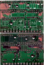
C3 and C7 are not on the same chip. They are in the signal path, one for the positive path and the other for the negative. If they are that much different, it may lead to a very unequal waveform, or it is justifed to make it equal. And bout C11, you just dont mention its value. It also seems that you dont have the same revison board as mine. Yours is 7 while mine is 6.
Do you found the burned component in yours? mine was both inverters that were shot.
Do you found the burned component in yours? mine was both inverters that were shot.
- Home
- Amplifiers
- Class D
- JBL PB12 subwoofer, Class D amp, dead.