H
HAYK
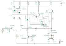

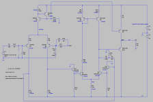
Looks like VAS transistors have EFs now. And input stage cascoded. What is the name of that compensation network?Look at this.
Another attempt to reduce parts count.
Hitachi amp.
No current mirror for the LTP.
Darlington pairs outputs.
At 1V input gives 0.0003% THD
60db NFB
Hitachi amp.
No current mirror for the LTP.
Darlington pairs outputs.
At 1V input gives 0.0003% THD
60db NFB
Attachments
Last edited:
H
HAYK
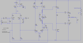
Magnificent, you can replace back Q5 with diode.
The compensation is the creation of @Rupopulles, I applied to the negative branch to liberate the positive capacitance and get very high slew rate 1kv/us.
The compensation is the creation of @Rupopulles, I applied to the negative branch to liberate the positive capacitance and get very high slew rate 1kv/us.
Exactly the simplified is hard to beat
you can fluff it and get down to .0003% in sim no problem.
Real life with power supply , load, preamp, ac coupling caps etc etc.
Its just plain good old .001% at 1k and .05% at 20k
Far as pushing it further. Most hole thru common transistors
work well. for the diff and vas. But to find higher performance
small signal transistors it would unfortunately be SMD.
Far as the extremely well gone over single vas topologys.
to get real world .001% the parts count is much much higher.
1ma is about right for the diff, I have got it down to 500u
which makes it extremely stable and very minimal degen.
So possible with minimal degen you guys can come up with
fancy compensation to extend the 20 K open loop stuff.
otherwise real life. PSRR is likely the bigger benefit.
Using slightly better current source or usual rail stuff
to keep a amp quiet. Or getting slew rate up with
better SMD components
Last edited:
correct they are easier to drive so dont need triple or EF3.
Just the usual tradeoff, higher idle current and loose about
5 / 6 volts of the rail.
All in all not too bad Mosfet have good safe operating area.
You can add a lot of output devices, so it could drive
4 ohm loads really well with 2 even 3 pairs.
Played around with both, its fun.
This topology has been a favorite among many for
mosfet and BJT and even overbiased fake class A.
been meaning to try all KSA/C 992 / 1845 for hole
thru. Otherwise maybe explore some Toshiba SMD
Last edited:
I have found this MPSA92 smd version PZTA92T1G - it should be able to dissipate up to 1W
Also FJV992 with hfe=500
Pretty much was on the bucket list to find
equal or better transistors from original circuit.
2SA872 pnp diff
then 2SB/D 716 / 756 for Vas
and 992 was one of them, could be others
equal or better transistors from original circuit.
2SA872 pnp diff
then 2SB/D 716 / 756 for Vas
and 992 was one of them, could be others
What if I add EF to VAS transistors? Will that drastically improve on thd? Or not worth it?Its just plain good old .001% at 1k and .05% at 20k
I am thinking about simulating input stage isolated from the output
so I can compare by adding small increments and running sim on thd and other metrics
Meanwhile, did mosfet version. Even less parts. Gets 0.00015% thd at 1V input, goes up to 0.0008 with 3V input.
Only 10 transistors.
~58dB NFB, but that's the best that can be done.... I feel like laws of physics come in at this point...
Area of concern is R20 dissipating fair amount of heat.
Lowering VAS current breaks the whole thing.
Not sure if there is any other solution, except using 0.5W or 1W rated resistor.
Attachments
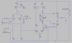
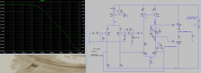
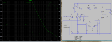
Just for fun added EF to VAS
Gets 0.00013% THD with 1V and with 3V input signal
Bode plot comfortably sits above 70+dB at 20kHz
Seems like helps to balance power dissipation (current???) in Q7 and Q8 transistors.
Gets 0.00013% THD with 1V and with 3V input signal
Bode plot comfortably sits above 70+dB at 20kHz
Seems like helps to balance power dissipation (current???) in Q7 and Q8 transistors.
Attachments
Last edited:
H
HAYK
2k load is too low. If you have 2EF each Hfe100, 8 ohms is 80k ohms. Much higher if MOSFET.
You can also try bootstrapping R4,R5 by linking to R16,R18 instead of ground.
Running the input transistors with 400ua bias A992 are better suited. OR, run at 2ma with more degenerated emitters.
You can also try bootstrapping R4,R5 by linking to R16,R18 instead of ground.
Running the input transistors with 400ua bias A992 are better suited. OR, run at 2ma with more degenerated emitters.
Last edited by a moderator:
I just realized I was trying the same amplifier.
Is R17 500 Ω fixed or a variable resistor?
And why did you change the BD's to KS's? What were you able to improve with this change?
Thanks
Is R17 500 Ω fixed or a variable resistor?
And why did you change the BD's to KS's? What were you able to improve with this change?
Thanks
- Home
- Amplifiers
- Solid State
- JAT501 simulated using TINA TI and possible improvements