Fundamental issues here. I mean, if the goal is to create a "real" amplifier circuit with real actual components. There are different types of mosfets. They have different properties. They have to be used properly in order to function correctly, depending on the application. Generally you have lateral and vertical. Also there are different vertical type architectures. One cannot just place any transistor to any function and expect it will magically work. It appears there needs to be more research committed to.🙄
You must be joking. If you have no clue other than the amplifier makes loud sound, then there is little or no bias current if it seems cold. If you try to increase the current to that recommended for the Darlington transistors though, you have no facility like emitter resistors to measure it and you will need to estimate from the total circuit idle current. Your bias control circuit likely doesn't have enough voltage drop to generate the correct bias for Darlingtons, which in case you weren't aware, probably have a lot more inside than just 2 BJTs.Mine works perfect.
I heated up a lot and there is no thermal runaway.....I was 😱 that the heatsink was COLD. Only very little warm. very very little
Maybe this is from the bootstrapping. 😎
For goodness sake, arrange the circuit to test the bias current after startup and immediately after playing a while - read up and at least learn what makes a proper circuit design from simple examples, before bombarding the forum with a load of half-baked ideas and omissions. A gadget that plays music is a start but how does it perform? Does it have correct and stable bias? Steady temperature at idle? Is the distortion harsh at low levels? Does it clip acceptably? Does it have slight HF oscillation? Full audio bandwidth?
If you are going to try to design electronic devices by trial and error, you are in for a lifetime of failure. You can use student Multisim to draw and test the steady-state of amplifier circuits but it will be useless for practical amplifier design where dynamic load changes and factors like heating, instability, safe operation and protection from typical forms of abuse is involved.
Many here are professionals whose business it is to read a schematic and likely problems with certainty- it's their job. We aren't just out of high school so we can help with most design issues and practical choices too but first start correctly with the basics yourself - a good book of theory and practical building as previously stated, read and study ESP website etc. It's all free if you have no cash but can obviously afford a PC and the internet fees, so look carefully, there are no excuses if you really want to learn about analog audio electronics, as we might hope in this Forum.
Last edited:
No Im not joking, and there is 73ma bias current measured between emitters.You must be joking. ...and you will need to estimate from the total circuit idle current.
I dont think so and think u all are in big error here. U all think that darlingtons voltage drop is double because of the two transistors, but its not !Your bias control circuit likely doesn't have enough voltage drop to generate the correct bias for Darlingtons, which in case you weren't aware, probably have a lot more inside than just 2 BJTs.
For goodness sake, arrange the circuit to test the bias current after startup and immediately after playing a while - read up and at least learn what makes a proper circuit design from simple examples, before bombarding the forum with a load of half-baked ideas and omissions.
There is only one voltage drop, because currents flows through the first emitter to the second via resistor !!! Then another current helps from first collector.

My bias voltages are exactly +-890mV. Bias current 73mA.
I am not hearing any distortion at all volumes.If you have no clue other than the amplifier makes loud sound. Is the distortion harsh at low levels? Does it clip acceptably? Does it have slight HF oscillation? Full audio bandwidth?
I havent tested clipping, there is no HF osc.
i hear full audio bandwidth but dont know actually, im only half AC analys.
however its better for the HF than my Mosfet one.
Its LF are more better too, very beautyfull LFs.
No im definately not. I know what im doing.If you are going to try to design electronic devices by trial and error, you are in for a lifetime of failure.
You are too insideYou can use student Multisim to draw and test the steady-state of amplifier circuits but it will be useless for practical amplifier design where dynamic load changes
I dont think it must that hard to analys dynamic load changes..
it must be just middle hard. not too hard.
I think all of u will use my vbe improvement.and factors like heating, instability, safe operation
I will test it reallife with bias current measure at high temperature.
But im sure it works because there wasnt thermal runaway @ extreme heats with the small heatsink. And yes I belive my sim's Thermal vs. Current graphic.
I improved my vbe even more, now using a resistor instead the second diode.
protection .. next time . now im carefull to not shortcircuit or overload.and protection from typical forms of abuse is involved.
actually im thinking of attaching a 50hz transformer to the output to
"feel" the music touching at the HV. Ofc i will measure to not be too dangerous.
Many here are insiders, i dont know what im doing here.Many here are professionals whose business it is to read a schematic and likely problems with certainty- it's their job. We aren't just out of high school so we can help with most design issues and practical choices too but first start correctly with the basics yourself - a good book of theory and practical building as previously stated, read and study ESP website etc. It's all free if you have no cash but can obviously afford a PC and the internet fees, so look carefully, there are no excuses if you really want to learn about analog audio electronics, as we might hope in this Forum.

You are too inside
I dont think it must that hard to analys dynamic load changes..
it must be just middle hard. not too hard.
Opps i missed a "be" after "must", I think there is no need for dynamic load analys..
This is only for insiders because it must be easy, not hard.
Dynamic load changes, blabla..
Anybody thinked about double bootstrapping ?
I think there is no better driving than this !!!!
i learned ltp and going to sleep for tommorow fun.
This is with 1-2 mA standby bias !!!
Today i mproved my darlington build by highering the bias to 200ma. It was very beutyful.
I think this will be MORE MORE SURPRISING, ASTONISHING.
Ive never seen symetrical bootstrapping but ITs a must.
For a cheapness or just want to save one Q you could change Q1 or Q2 with a resistor. 😀
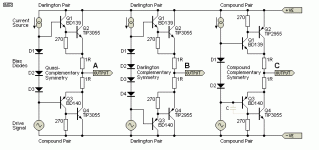
Output Q's are Darlingtons with max beta of 20000 !!!
P.S. Today I was wondering why my one transistor heated up more than the other 😀
Now I answered my question. Think about it 😉
It needs Simple symetry, not a "trick", and a trick 😀
magic is always paradoxical. you never know. only in diyaudio 😀
I think there is no better driving than this !!!!
i learned ltp and going to sleep for tommorow fun.
This is with 1-2 mA standby bias !!!
Today i mproved my darlington build by highering the bias to 200ma. It was very beutyful.
I think this will be MORE MORE SURPRISING, ASTONISHING.
Ive never seen symetrical bootstrapping but ITs a must.
For a cheapness or just want to save one Q you could change Q1 or Q2 with a resistor. 😀
Output Q's are Darlingtons with max beta of 20000 !!!
P.S. Today I was wondering why my one transistor heated up more than the other 😀
Now I answered my question. Think about it 😉
It needs Simple symetry, not a "trick", and a trick 😀
magic is always paradoxical. you never know. only in diyaudio 😀
Attachments
Last edited:
Anybody thinked about double bootstrapping ?
I think there is no better driving than this !!!!
Ive never seen symetrical bootstrapping but ITs a must.
Old news. Been used for decades...
One advantage is that it allows for use of smaller and faster transistors, for example, Driver or Pre-driver transistors.
Old news. Been used for decades...
One advantage is that it allows for use of smaller and faster transistors, for example, Driver or Pre-driver transistors.
And nobody uses it ?
Its awsome, lowers the Power dissip.
Maybe its beautyful to have a transistor in the output stage 😀 😱

What about this people think darlington have 1.4v drop ???
And use 4 bias diodes, this is silly. Also with quasi, they all must be same, 2
There is only one drop, the first via the 270ohm resistor to out
Attachments
Last edited:
Ok bootstrapping is a very bad idea. I found out.
Firstly i was testing without this symetry and i was looking only at the first transistor's Pd.
Look at the results, without bs -> less Pd and less distortion.
Maybe its good 0.007 with load, and maybe this is real 😛
P.S. Look at the third attach, +-36.368 output swing with +-36.5V supply voltage
Firstly i was testing without this symetry and i was looking only at the first transistor's Pd.
Look at the results, without bs -> less Pd and less distortion.
Maybe its good 0.007 with load, and maybe this is real 😛
P.S. Look at the third attach, +-36.368 output swing with +-36.5V supply voltage
Attachments
Last edited:
There is only one drop, the first via the 270ohm resistor to out
No.
You have no argument, explain.
When voltage is 0.7 Q1 starts conduction and current flows from its collector to the 2nd base, this current is with voltage of supply voltage.
Look @ ur signature: "If you can't explain it simply, you don't understand it well enough (c)"
When voltage is 0.7 Q1 starts conduction and current flows from its collector to the 2nd base, this current is with voltage of supply voltage.
Look @ ur signature: "If you can't explain it simply, you don't understand it well enough (c)"
Last edited:
And but nobody uses it ?
Its awsome, lowers the Power dissip.
Personally, I like this approach. Bootstrapping CAN be a very good idea. Have trouble finding suitable driver transistors that are fast and have good current handling. One option is to use cascoded drivers but I prefer the bootstrapped arrangement.
You do have consider the potential stability issues with feeding back the amplifier output to the collectors of the bootstrapped transistor.
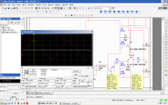
Ahh, its good, i found out when i pushed the ops to its limit just before clipping.
Look at it, 111.070W @ 6ohm with Pd 15.5W per transistor.
And this is not the peak, this means 290W peak, 41W peak Pd per Transistor.
Is this means i have to use 340-50W transformer ?
Maybe i'll stick with the opamp 😀
I think this will be a nice successful build. 😉
These darlingtons are 70-80W and maybe i need my other transformer which is not here. Its +-50V.
Without bootstrapping, some killowats Pd and A lot of distortion 😀
Attachments
Last edited:
You have no argument, explain.
When voltage is 0.7 Q1 starts conduction and current flows from its collector to the 2nd base, this current is with voltage of supply voltage.
Look @ ur signature: "If you can't explain it simply, you don't understand it well enough (c)"
That's very easy to explain - you can find the explanation in any book on transistor basics.
In order for the transistor to work in the linear region (transistor is open, collector current is not zero), it has to be properly biased (Vbe has to be applied).
In Darlington arrangement you've got 2 base-emitter junctions in series, so you need 2 x Vbe for them to open. The fact, that the 2-nd base-emitter junction is shunted with a resistor does not change anything - that resistor just increases the 1-st transistor's (driver's) collector current (increasing linearity).
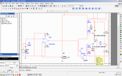
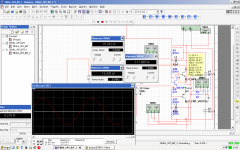
See a simulation fragment of the working circuit. Each Vbe = 0.55V (roughly). Power transistors' bias is slightly lower than average (0.55V instead of 0.65V).
Is it... sort of... clear?
Attachments
No, without this resistor is like you said.
With it is like i said in my post (the same here), just because the first transistor starts conducting through this resistor and allows conduction of the second @ only 0.7V.
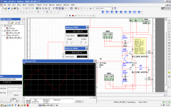
P.S. smb explain me what is Ta and what is Tc in the 2nd attach, the difference ?
thank you.
With it is like i said in my post (the same here), just because the first transistor starts conducting through this resistor and allows conduction of the second @ only 0.7V.
P.S. smb explain me what is Ta and what is Tc in the 2nd attach, the difference ?
thank you.
Attachments


Last edited:
With it is like i said in my post (the same here), just because the first transistor starts conducting through this resistor and allows conduction of the second @ only 0.7V.
If - as you are saying - the first transistor starts conducting through the resistor, there is a voltage drop over that resistor. That voltage drop forms the second transistor's Vbe bias. And it's not 0.7V - it's less in practice, as I have already mentioned.
On your picture, you've got 1.4mA overall current with 1V overall bias. Your second transistor is closed completely - that 1.4mA goes through the first one only. Put the probes in the right places and see the collector current of each transistor (like I showed in the previous post).
You contradict yourself.
Within a number of threads you're trying to argue on things you don't know well enough with people who's everyday job is designing the circuits.
What's the purpose? 🙄
Personally, I like this approach. Bootstrapping CAN be a very good idea. Have trouble finding suitable driver transistors that are fast and have good current handling. One option is to use cascoded drivers but I prefer the bootstrapped arrangement.
You do have consider the potential stability issues with feeding back the amplifier output to the collectors of the bootstrapped transistor.
There's no trouble, look at these are good candidates -> http://www.st.com/web/en/resource/technical/document/datasheet/CD00000939.pdf
They are 40W and i think their freq is 10Mhz.
Datasheet says good hfe linearity and high ft frequency 😉
Im trying to catch smth ofcourse 😀If - as you are saying - the first transistor starts conducting through the resistor, there is a voltage drop over that resistor. That voltage drop forms the second transistor's Vbe bias. And it's not 0.7V - it's less in practice, as I have already mentioned.
On your picture, you've got 1.4mA overall current with 1V overall bias. Your second transistor is closed completely - that 1.4mA goes through the first one only. Put the probes in the right places and see the collector current of each transistor (like I showed in the previous post).
You contradict yourself.
Within a number of threads you're trying to argue on things you don't know well enough with people who's everyday job is designing the circuits.
What's the purpose? 🙄
smth tricky 🙄
And i catched it 😀 This bootstrapping technique. Its known but nobody uses 😉
Im going to make a very powerfull amplifier with just these little plastics -> http://www.st.com/web/en/resource/technical/document/datasheet/CD00000939.pdf
I missed the part current comes from the first, I thinked the 2nd base sees the full voltage but its only in the mv range ..
--
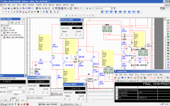
Look at my part list 😀
47 ohm
470 ohm
1k
47uF 25V
47uF 50V
tenol
kabel
cokli
konektori
bd677
bd678
bd679
bd680
bd681
bd682
bd683
bd684
TIP122
TIP110
BDX53C
BDX54C
--------------
BDX33C
Last edited:
There's no trouble, look at these are good candidates -> http://www.st.com/web/en/resource/technical/document/datasheet/CD00000939.pdf
They are 40W and i think their freq is 10Mhz.
Datasheet says good hfe linearity and high ft frequency 😉
Depends on what you call fast. 10Mhz isn't fast. For Driver transistors I look for ft of 100MHz+ hence my liking of bootstrapping. Along with using MOSFETs for the output transistors. Faster transistors mean better stability margins for a given ULGF.
The best i can get it:
The distorsion is very low at low power.
I will try to use these mentioned as output transistors.
I think im going to out 12-13W with these.
they are very very cheap -> 0.15 euro
If i parallel them ,I can easily get 50W.
The distorsion is very low at low power.
I will try to use these mentioned as output transistors.
I think im going to out 12-13W with these.
they are very very cheap -> 0.15 euro
If i parallel them ,I can easily get 50W.
Attachments
Last edited:
- Status
- Not open for further replies.
- Home
- Amplifiers
- Solid State
- Is this good ?