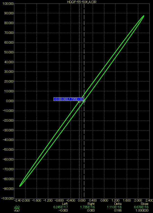
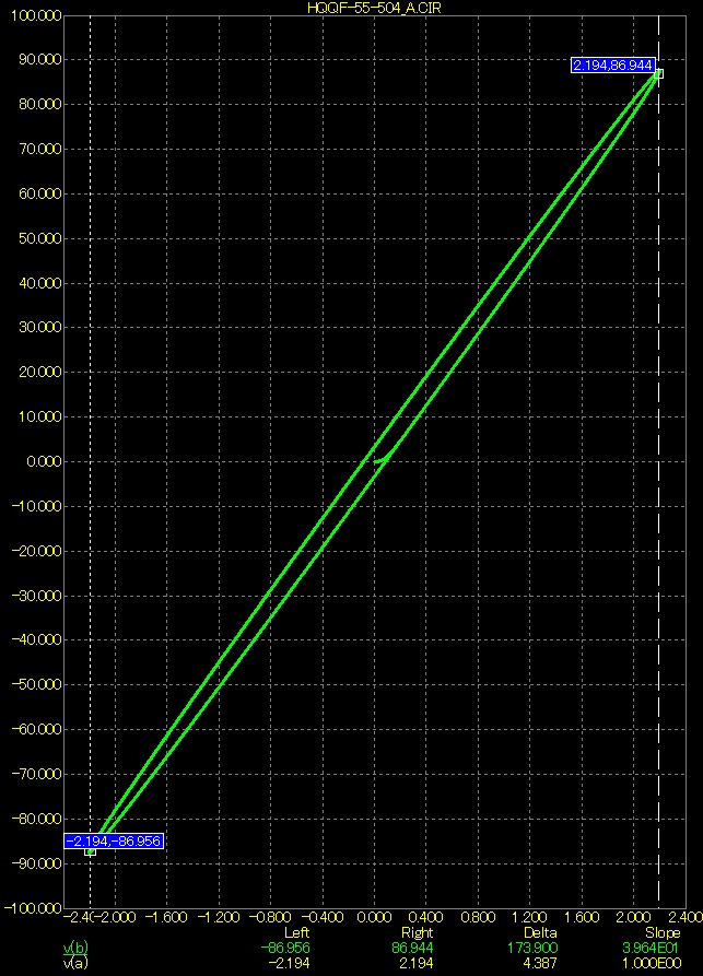
The result is not very good. It is good to 50V, there is Vdif 2x24mV. When the output voltage of 86V is Vdif 83mV and it is very much.
That's nice, Federmann...and with output mosfets ?
"And with output MOS-FETs" No worries, the result is very similar.
The result is not very good. It is good to 50V, there is Vdif 2x24mV. When the output voltage of 86V is Vdif 83mV and it is very much.
Federmann,
Vdif is the effective input signal. Of course, if you increase the output voltage, Vdif MUST rise in proportion (within the linear range of the amp).
So if your Vdif is 46mV with 50V output, that shows an open loop gain of just above 1000. (Actually 1087 exactly). With 86V out, and the same open loop gain, I would expect a Vdif of 86/1087 = 80mV. That's close enough to your measured 83mV I would think.
jd
Amplification stages are not linear. Greater Vdif represents a decrease gain.
2 x 24mV = -10%
83mV = approx -20%
48mV, the third harmonic output voltage 10%, 1% output power.
83mV, the third harmonic output voltage 20%, 4% of output power.
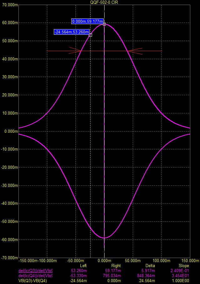
Open loop, gain decreases the frequency but also decreases the size of the output voltage, accurately the size of Vdif.
Open loop, gain decreases the frequency but also decreases the size of the output voltage, accurately the size of Vdif.
Correct. The gain decreases slowly with increasing output voltage. I just didn't want to bring that secondary effect into it yet. It's called gain compression.
Since the OL gain also rolls off with frequency, you will also see the Vdif increasing in ratio with frequency. ALL amplifiers will show this to varying degrees, as I'm sure you know.
jd
The precise setting Vdif without a signal, using P - I controller, everything is much better.
Not sure I follow you. The only Vdif without signal is the DC offset.
jd
"P - I controller"Not sure I follow you. The only Vdif without signal is the DC offset.
Yes, he means DC servo, to hold conditions in the midlle of linear region, and he is believing this should improve also hf linearity..
"P - I controller"
Yes, he means DC servo, to hold conditions in the midlle of linear region, and he is believing this should improve also hf linearity..
Ahh yes, thanks!
jd
On second thought, adjusting Vdif with a PI controller to get zero DC at the output would generally move the input diff pair away from it's linear middle part of the transfer. That doesn't seem a good career move 😉
jd
jd
That doesn't seem a good career move 😉
jd
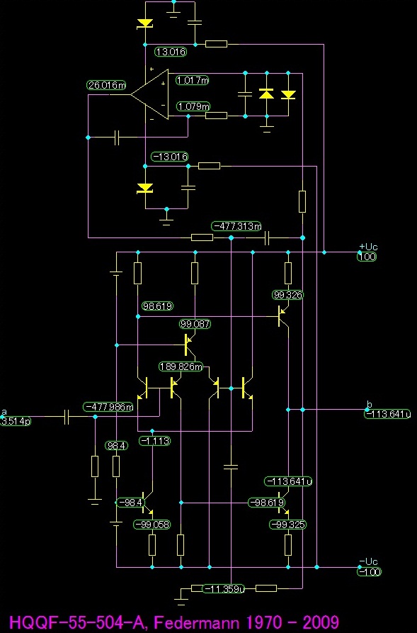
The voltage unbalance and current. The main share of the output voltage error does input current unbalance. The base resistance large , there is a large deviation.
The voltage unbalance and current. The main share of the output voltage error does input current unbalance. The base resistance large , there is a large deviation.
Hmmm. I don't think it matters whether you characterise the unbalance as current or voltage unbalance. The important point is that if you unbalance the input pair, you move to a more non-linear region.
jd
Any change in parameters of the second stage is reflected in the setting of the first degree. Are intertwined issues. Basis-are 47kΩ resistors.
PI controller adjusts Vdif close to 0V, when the temperature changes and changes in supply voltage.
Dc servo sets the zero voltage output, nothing more.
Dc servo doesn't know what is needed Vdif.
Dc servo doesn't know what is needed Vdif.
Dc servo sets the zero voltage output, nothing more.
Dc servo doesn't know what is needed Vdif.
0V output voltage is derived from Vdif.
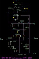
Federman, I've added part numbers to your schematic to illustrate.
Assume that Vbe(Q1)=Vbe(Q2)
Assume that Vbe(Q3)=Vbe(Q4)
Assume that for any transistor Vbe increases with Ic.
Following this, Vdif will be equal if and only if Ic(Q1)=Ic(Q2)=Ic(Q3)=Ic(Q4).
So, say Ic(Q1) is not equal to Ic(Q2), and this causes Vdif to be -2mV.
The servos will add 2mV to the base of Q2, but the base of Q1 will still be 0V.
So you see that the real problem is the Ic of the LTP's.
Ic(Q1) roughly equals Vbe(Q5)/R2.
Ic(Q3) roughly equals Vbe(Q6)/R1.
So really the only way to minimize Vdif is to:
1: Adjust R2 until Ic(Q1)=Ic(Q2)
2: Adjust R1 until Ic(Q3)=Ic(Q4)
3: repeat until both LTP's are balanced
After doing this there should be no need for a servo since, as you say, Vout is derived from Vdif.
- keantoken
Attachments
Sorry to butt in, but would you be so kind as to look there, it may (just) be interesting in your discussion:
http://www.diyaudio.com/forums/software-tools/158209-spice-transistors.html#post2039975
http://www.diyaudio.com/forums/software-tools/158209-spice-transistors.html#post2039975
- Status
- Not open for further replies.
- Home
- Amplifiers
- Solid State
- Influence of the delay amplifiers for listening characteristics