I'm sure your measurement system is fine. Why did you type that info - I never questioned it.
//
//
You did ask about the setup so I meant the measurement setup.
If you mean the DUT setup it was the FifoPi stacked on the RPI 3 with Crystek and TWTMC-DRIXO at 22/24 MHz.
If you mean the DUT setup it was the FifoPi stacked on the RPI 3 with Crystek and TWTMC-DRIXO at 22/24 MHz.
By that I mean how the DUT was setup.
OK - and the rest? How was things connected?
A picture?
//
OK - and the rest? How was things connected?
A picture?
//
Sorry, I have no pictures, it was some months ago.
However the Crystek oscillators were installed as suggested from the designer with his adapter boards and powered by low noise linear regulators.
The Driscoll oscillators were installed using the TWTMC-STS-SX and TWTMC-STS-DX sine to square converter boards that fit the FIfoPi board, and powered by the TWRPS-UGL linear regulators as in the attached PDF.
Attachments
Yes, but the ring DAC works in a different way, it's not a 1 bit DAC, it uses a ladder network and the signal turns around the ladder so the tolerance of the resistors is averaged.
However the DAM1021 is a PCM DAC, so what happens in a PWM DAC does not matter.
The better inherent linearity of a PWM DAC is true, pity that they are real noise generators.
But it's a question of point of view.
I've got a couple DCS AD converters that use the principle. They do produce more realistic dynamics and natural high end than any delta sigma ADC I've tried, including those as pricy as the the DCS converters.
Thanks - now just missing where measurement probe where attached. Sorry for calling i "measurement setup" when actually meaning "test setup" i.e. both DUT and measurement equipment combined.
I simply still cant connect the 3 different traces (blue, magenta and green) to what was measured in what configuration. Naming isn't helping me... Sorry.
You would have:
a source: RPI
an output: RPI fifo
a fifo with clock: Crystek or andrea
the andrea clock
The DUT configs:
a) RPI -> RPI fifo with Crystek -> clock-out(a)
b) RPI -> RPI fifo with andrea clock -> clock-out(b)
c) RPI -> clock-out(c)
d) andrea clock -> clock-out(d)
Can you connect clock-out(a)....(d) to the B(lue), G(reen) and M(agenta) graphs in the Ian post #5423 if at all the variants exist in the list above, please?
I assume measurement probe is connected to clock-out(a)....(d) respectively.
I assume that (a) and (b) was measured on the clock output of the fifo.
//
The DUT configuration you have listed is OK.
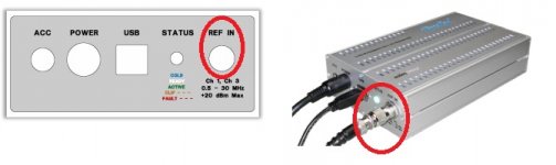
The DUT input of the Timepod was connected via u.fl to SMA cable and 6 dB attenuator to:
- FifoPi with Crystek MCK u.fl output (blue trace of the second picture)
- FifoPi with Crystek SCK u.fl output (green trace of the second picture)
- RPI I/O header BCK via SMA adapter (magenta trace of the second picture)
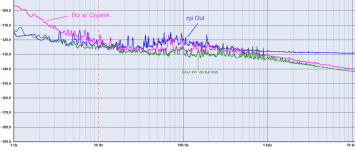
- FifoPi with Crystek LRCK u.fl output (green trace of the third picture)
- RPI I/O header LRCK via SMA adapter (magenta trace of the third picture)
- FifoPi with Driscoll MCK u.fl output (magenta trace of the fourth picture)
- FifoPi with Driscoll SCK u.fl output (green trace of the fifth picture)
- FifoPi with Driscoll LRCK u.fl output (green trace of the sixth picture)
The last plot compares:
- FifoPi with Crystek LRCK u.fl output (magenta trace)
- FifoPi with Driscoll LRCK u.fl output (green trace)
- RPI I/O header LRCK via SMA adapter (Blue trace)
The DUT input of the Timepod was connected via u.fl to SMA cable and 6 dB attenuator to:
- FifoPi with Crystek MCK u.fl output (blue trace of the second picture)
- FifoPi with Crystek SCK u.fl output (green trace of the second picture)
- RPI I/O header BCK via SMA adapter (magenta trace of the second picture)
- FifoPi with Crystek LRCK u.fl output (green trace of the third picture)
- RPI I/O header LRCK via SMA adapter (magenta trace of the third picture)
- FifoPi with Driscoll MCK u.fl output (magenta trace of the fourth picture)
- FifoPi with Driscoll SCK u.fl output (green trace of the fifth picture)
- FifoPi with Driscoll LRCK u.fl output (green trace of the sixth picture)
The last plot compares:
- FifoPi with Crystek LRCK u.fl output (magenta trace)
- FifoPi with Driscoll LRCK u.fl output (green trace)
- RPI I/O header LRCK via SMA adapter (Blue trace)
"The DUT input of the Timepod was connected via..."
did you mean:
The DUT output was connected to the Timepod via..
?
//
did you mean:
The DUT output was connected to the Timepod via..
?
//
This raises a few questions…
- What clocks are on the RPI itself (not the RPI fifo!)? It looks very good below 10Hz! Is it really possible??
- Acc to you a DAC would be better off being fed directly by a RPI than a fifo with Crystek due to better close-in performance!
- All would be explained if the intrinsic jitter of the fifo logic (ideal clocks) was according to the red line (see pic below).
- We see the fifo helping for RPI out. No traction between in and out pn — see blue and magenta deviating! fifo works as long as fifo clock is better!
- We see that adding a better fifo clock (andrea) do not gain anything much as the limit of the pn floor is set by fifo itself, not fifo clock.
Attachments
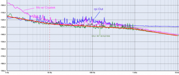
1) the RPI uses a 19 MHz VCXO and a PLL to generate I2S, it's not a good oscillators.
But keep in mind that the masterclock is divided down several times to get the LRCK and theoretically the phase noise improves 6 dB for division.
2) never tried both option so I don't know. However I would use a well isolated FIFO buffer to avoid source dependance
3) I don't know what happens inside the FIFO, but keep in mind that the Driscoll has at least 30 dB less phase noise than the Crystek
4) it's obvious! but the phase noise of the Driscoll is better than the LRCK Fifo output while should be the opposite since we are dividing down the master clock
5) isolation issue, there is a clear crosstalk. The LRCK should come directly from the master clock without crossing the FPGA
The road to updating
Let examine a little how the DAC of the DAM1021 works in order to better understand the possible upgrade.
Substantially there are 8 x 74LVC595 shift registers/latches and double ladder network for each channel.
Since the digital to analog conversion is done with sign magnitude notation there are 2 x 27 bit ladder networks, one for the negative portion of the output signal and the other for the positive one. The two 27-bit ladder networks allow to get a 28-bit DAC.
This way requires the switches (LVC595) to be doubled to operate with bipolar power supply.
Indeed the upper 4 x LVC595 are connected to the negative power supply to treat the negative part of the output signal, while the lower 4 x LVC595 are connected to the positive supply rail.
Actually the GND pins of the upper banks are connected to -4V and the VCC pins to ground, while the GND pins of the lower banks are connected to ground and the VCC pins to +4V.
In order to avoid short circuit between the two ladder networks the Output enable pins of the 595s have been used.
The output enable pins of the upper 595s are driven with a signal opposite to the lower ones.
When the output of the 74LVC595 is disabled it goes in high impedance state, so only the upper or the lower switch banks are connected to the ladder network at a moment, while the opposite banks are in high impedance state and therefore disconnected from the ladder network.
Since the upper and the lower 595 banks are connected to a different voltage reference they have to be driven by signals referenced to the same reference of each bank.
In other words the voltage swing seen by the upper banks has to be from -V and ground, while the voltage swing seen by the lower banks has to be from ground to +V.
Keep in mind that the voltage swing from the I/O ports of the FPGA is from ground to VCC (in this case 3V3 single ended) therefore it's suitable to drive correctly the lower 595 banks but not the upper banks.
There are several ways to drive the 595 banks with bipolar signals starting from a unipolar signal like the one from the FPGA, in the DAM1021 was chosen the simpler way: AC coupling.
Indeed every signal coming from the FPGA is decoupled using a capacitor.
LRCK and DATA have also a pair of resistors on the 595 input pins. These resistors set the the input pins of the LVC595 to half VCC, around -2V (one resistor is tied to -4V and the other to ground) for the upper banks and +2V (one resistor is tied to +4V and the other to ground) for the lower banks.
Conversely the BCK input of the 595s has no pull resistors, AC decoupling only.
This difference of driving is due to the features of the managed signals.
The bit clock is a continuous signal at relatively high speed while the LRCK is still a continuous signal but at lower speed. Finally the DATA signal is not a clock signal since it can assume 0 or 1 values for a long period, theoretically much longer than the LRCK cycle.
Therefore the AC coupling capacitor has to keep the voltage at the same logic level of the incoming signal until its state is changed.
Even a small size capacitor does easily the job with high speed clock signal like the bit clock.
But with low speed clock like the LRCK or with non clock signal like the DATA a single capacitor could become an issue because the logic level could change after a long period.
Therefore the pull resistors have been added to avoid the quick capacitor discharging in order to keep the logic level for longer time.
Practically the voltage level of the LRCK and DATA input pins are biased at half VCC (+2V and and -2V) and thanks to the AC coupling the incoming signals from the FPGA swing from -1.65V and +1.65V.
This means that the input pins of the upper 595 banks see a voltage swing from -3.65V and -0.35V and the 595s of the lower banks see a voltage swing from +3.65V and +0.35V .
The above voltage values are suitable to get the 595s to switch correctly since they are compliant with the treshold voltage of the device needed to change the logic level (with 3V3 VCC the HIGH-level input voltage is 2V and LOW-level input voltage is 0.8V).
This way is simple and cheap (a few resistors and a few capacitors) but has a disadvantage: the clean signal like the LRCK share the same ground of the dirty signals (data and bit clock).
Not the best isolation since they are RF signals and could be mixed on the PCB generating crosstalk and noise.
The measurements will tell.
I have not clear how have been managed the OE inputs of the 595s used to select the appropriate banks as function of the sign, maybe I will take a look with the oscilloscope as soon as I have powered on the DAM1021.
However it's not an issue in order to implement the upgrade because just removing the resistors before the OE pins (before ENN and ENP in the schematic) to get the 595s disconnected from the FPGA.
In conclusion 36 capacitors and 4 resistors have to be desoldered to install the interface board in order to get the DAC fed by a true FIFO buffer with fixed oscillators.
I spent quite a lot of money and time on this. I will see how it pans out first.
Did you try distributing the clock from a single DAM to all the others (removing the VCXO from all the others)?
Did you try distributing the clock from a single DAM to all the others (removing the VCXO from all the others)?
No. Is that so easily possible? In that case I'd rather remove all of them and use an ultra low jitter clock to feed all the DACs.
I think it could be possible but the designer should help.
The DAM1021 uses the PLL of the SI514 to track the input frequency, I believe that the micro reads the input clock and then it adjust the frequency of the VCXO via I2C and then it clocks the FPGA with the adjusted frequency.
This is a feedback mechanism that cannot be avoided to get the DAM working.
So the designer should provide infos about this feedback to understand what signals you have to distribute, I believe that the output clock only is not enough.
As I said several times the DAM1021 is sold as a diy products so I believe that the designer should help a little to manage typical diy updates, although without the disclosure of the design.
However you cannot replace the SI514 of all DAC with a fixed oscillator because at least the master DAM needs that VCXO to implement the feedback mechanism.
Maybe you can replace the SI514 of the master DAM with the SI570, they should share the same footprints and functions.
Please, try to ask the designer.
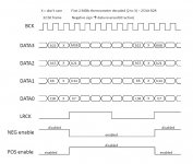
The most critical signal for a PCM DAC like the DAM1021 is the LRCK because it provides the latch to the switches.
In other words this is the precise moment when the data loaded into the registers update each bit of the ladder network (one or more bit depending on the incoming data word).
Therefore the bit clock is not so critical because the only purpose is loading data into the shift registers and so the quality of the clock does not matter.
Although the OE is even important it's not as critical as the LRCK, because it changes its logic level at zero crossing only, and usually a few LSBs are active in that moment (maybe all bit are zeros).
- Home
- Source & Line
- Digital Line Level
- Implementing a true FIFO buffer with low phase noise clock on the Soekris DAM1021 DAC