Both options are natively supported in their hardware: PCM and DSD
Well, in ring DAC hardware configuration (DSD PWM) the error in the ladder can be cured a little averaging the tolerance of the resistors.
In PCM DAC hardware configuration nothing can be done to cure the error in the ladder, the accuracy depends exclusively on the tolerance of the resistors (and on the casuality of their combination).
Last edited:
That's another thing.
Maybe we will provide the option of a one time calibration of the DAC to be used in the FIFO Lite to correct the resistors error.
I don't know, we will decide after listening sessions.
However it will be a one time calibration, not a continuous calibration like the one would seem to be implemented in Soekris DAC.
This is another way to generate noise.
Ok, but if it will be provided our option is one time calibration.
We have no intention to install a ADC on the DAC or on the FIFO boards, moreover it should be as good as the DAC.
And we see no reason to make the calibration more than one time.
BTW, as I said I don't know if we will provide this option.
We have no intention to install a ADC on the DAC or on the FIFO boards, moreover it should be as good as the DAC.
And we see no reason to make the calibration more than one time.
BTW, as I said I don't know if we will provide this option.
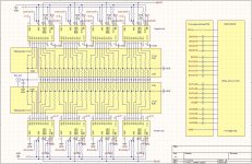
The following pictures are:
- DAC schematic (switches and ladder network)
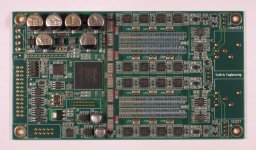
- DAM1021 PCB with the highlighted parts to be desoldered in order to install the interface board (36 capacitors and 4 resistors)
Next posts I will explain the update.
- DAC schematic (switches and ladder network)
- DAM1021 PCB with the highlighted parts to be desoldered in order to install the interface board (36 capacitors and 4 resistors)
Next posts I will explain the update.
Attachments
Last edited:
I have measured the phase noise of the clock signals before and after the FIFO. Although there is a clear improvement the curves are somewhat related, like if something from the input was reflected to the output.
That's really interesting. Do you have graphs you can post?
One way to completely decouple the clocks would be to use an asynchrous protocoll and wireless transfer.
You can find the measurements at this link
Asynchronous I2S FIFO project, an ultimate weapon to fight the jitter
Asynchronous I2S FIFO project, an ultimate weapon to fight the jitter
Interesting, thanks!
Looking at your above schematic, are the LRCKXX clock signals all the same LR clock signal? If so, wouldn't it be possible to let the FPGA do it's thing, unsolder only the 8 LR clock caps and feed a low noise clock to the 8 ladder inputs as well as to the source? Since the clock is a highly stable periodic signal I assume the delay of the FPGA would not really matter, but maybe a permanent misalignment would have to be corrected, by introducing a minimal delay (maybe with an allpass-filter/phase shift circuit kind of thing)?
Looking at your above schematic, are the LRCKXX clock signals all the same LR clock signal? If so, wouldn't it be possible to let the FPGA do it's thing, unsolder only the 8 LR clock caps and feed a low noise clock to the 8 ladder inputs as well as to the source? Since the clock is a highly stable periodic signal I assume the delay of the FPGA would not really matter, but maybe a permanent misalignment would have to be corrected, by introducing a minimal delay (maybe with an allpass-filter/phase shift circuit kind of thing)?
You can find the measurements at this link
Asynchronous I2S FIFO project, an ultimate weapon to fight the jitter
Is it post #5423 in that thread? Please talk me through what you have identified in terms of carried over jitter/pn. State which picture, color graph and observation.
//
Interesting, thanks!
Looking at your above schematic, are the LRCKXX clock signals all the same LR clock signal? If so, wouldn't it be possible to let the FPGA do it's thing, unsolder only the 8 LR clock caps and feed a low noise clock to the 8 ladder inputs as well as to the source? Since the clock is a highly stable periodic signal I assume the delay of the FPGA would not really matter, but maybe a permanent misalignment would have to be corrected, by introducing a minimal delay (maybe with an allpass-filter/phase shift circuit kind of thing)?
To do this the FPGA should be slaved to the external LRCK.
It's exactly what we have made in the FIFO Lite.
Unfortunately this way cannot be implemented in the DAM1021 because FPGA and micro firmware should be rewrite.
Therefore the designer only could make the job, but it looks like he had no intention since I suggest him this way several years ago.
Is it post #5423 in that thread? Please talk me through what you have identified in terms of carried over jitter/pn. State which picture, color graph and observation.
//
Please take a look at the picture number 8 (08 fifopi-lrck-rpi-crystek-driscollxo-att6db-png.png).
The LRCK output from the FIFO is almost superimposable to the LRCK input from the RPI.
Although the phase noise of the master clock is much better and the LRCK output is divided down from the master clock, that means theoretically 6 dB better each division.
Thanks. OK, I cant sort out the measurement setup so I cant make a judgement. I remember when I saw these - to much information missing or unclear for me in order to get something out of them. A drawing would have been nice. What is MTI260?
A fifo buffers job is to enable replacement of a poor clock with a better clock - right?
You write in your thread #2403:
"If you look at the SCK output comparison plot you can see that the SCK is 8-9 dB better than the original from the RPI with the Crystek, and 22-23 dB better with the Driscoll at 1 Hz from the carrier.
At 10 Hz from the carrier the SCK output has almost the same phase noise of the RPI, while it's almost 16 dB better with the Driscoll."
Seems it works - no?
//
The phase noise analyzer used is the Timepod 5330A (it uses cross correlation) and the measurements were done in 3-cornered hat configuration (with 2 reference oscillators).
This way allows measuring DUT with better phase noise than the reference.
The MTI260 are the 5MHz OCXO used as the reference.
Yes, it does work but not as expected since the master clock oscillator has far better phase noise than the FIFO outputs and the division should improve the phase noise.
This means that something does not work properly in the FIFO, maybe it's a isolation issue.
I cannot say about since I don't know harware and software design choices.
For sure there is a huge crosstalk on the LRCK output.
This means poor isolation between LRCK and BCK.
Difficult to say where the crosstalk coming from.
Well, in ring DAC hardware configuration (DSD PWM) the error in the ladder can be cured a little averaging the tolerance of the resistors.
Andrea a true DSD / PWM pulse array DAC doesn't work that way. The resistors
do not need to be accurately matched to achieve low distortion and in fact
various low pass filter responses can be achieved with different resistor
weighting through paralleling. As long as a given 'bit' or resistors value doesn't
change it will not add distortion.
This is one reason PWM DAC has much better inherent linearity than R2R DAC.
TCD
....
Yes, it does work but not as expected since the master clock oscillator has far better phase noise than the FIFO outputs and the division should improve the phase noise. ...
Is this compared to a freestanding clock measured at the connector of the box as you build them and; to how it works when used in context i.e. used in by a FiFo and checking clock coming out to the DAC section?
//
Andrea a true DSD / PWM pulse array DAC doesn't work that way. The resistors
do not need to be accurately matched to achieve low distortion and in fact
various low pass filter responses can be achieved with different resistor
weighting through paralleling. As long as a given 'bit' or resistors value doesn't
change it will not add distortion.
This is one reason PWM DAC has much better inherent linearity than R2R DAC.
TCD
Yes, but the ring DAC works in a different way, it's not a 1 bit DAC, it uses a ladder network and the signal turns around the ladder so the tolerance of the resistors is averaged.
However the DAM1021 is a PCM DAC, so what happens in a PWM DAC does not matter.
The better inherent linearity of a PWM DAC is true, pity that they are real noise generators.
But it's a question of point of view.
Last edited:
Is this compared to a freestanding clock measured at the connector of the box as you build them and; to how it works when used in context i.e. used in by a FiFo and checking clock coming out to the DAC section?
//
Sorry, I have not understood the question.
The measurements have nothing to do with the DAC, we have measured the phase noise of the FIFO buffer.
OK - how would we know without a sketch of the setup?
What I ment by "coming out to the DAC section" was: out from the fifo. OK?
So the clock is 20 db better after the fifio than before - how is this not suppression?
Of course the clock will be squachd by electronics in the fifo - to the grade that both bad and good clocks look the same.
To convey your superb pn figures on the bnc contact from a clock to reach the a DAC where it does good will be a huge challenge...
Its the fifo degrading the pn, not pn being carried over?
//
Here you can find all the information about the 3-cornered hat measurement with the Timepod (although the doc is about the new PhaseStation the measurement tecnique is the same for both)
http://www.miles.io/PhaseStation_53100A_AN_53100A_2.pdf
About the phase noise degrading in the FIFO buffer I cannot say much, I have not designed the FIFO and I cannot access any hardware and software informations.
You should ask the designer.
http://www.miles.io/PhaseStation_53100A_AN_53100A_2.pdf
About the phase noise degrading in the FIFO buffer I cannot say much, I have not designed the FIFO and I cannot access any hardware and software informations.
You should ask the designer.
- Home
- Source & Line
- Digital Line Level
- Implementing a true FIFO buffer with low phase noise clock on the Soekris DAM1021 DAC