This means for SR 44.1kHz & 4M samples and higher sample count: To wait 1.5 Minutes to play 😱
Also, on lower samples as 1..2 minutes, some space management is required while getting a space, but still to play 4M samples 😀
Interesting for a side project:
. while the incoming I2S have to be converted to parallel for the FIFO RAM banks using a controller anyway or not?
. interesting would be to use the parallel interface with high xx MHz SR to sample from a fast ADC to the FIFO and reading with a known audio I2C to a lower SR SPDIF >> USB interface.
. May Fre and others may love it 😀
. But the maximal parallel input frq. should be known
. In other words as the DSO do
You have 2.9 seconds of latency so you wait 2.9 seconds to play (ooops... 1.45 seconds since the buffer was loaded to half capacity).
Last edited:
The strange world of DIY
It's very curious.
The DAM1021 was presented as a diy product on a diy audio forum.
Maybe some users got the board just to tweak it with minor or major updates, depending on the skills, on the budget and so on.
But when the user asks for infos about the board in order to make the tweaking the designer does not reply
Reference DAC Module - Discrete R-2R Sign Magnitude 24 bit 384 Khz
So the user, who have paid EUR 373.75 + shipping (EUR 299 + 25% VAT) for a diy product, has to waste time to get the infos by himself, using DMM, oscilloscope and so on (if he owns the gears).
It's not just the right behavior in the spirit of diy.
Think that John Curl and Nelson Pass share their designs and kindly answer to all the questions from the users!
I have already said my thought, there is something wrong.
Most of your boards are also finished. And you do keep sekrets due to your fellow designer doesn't let you expose some the secret sauce. But nothing was promised I suppose...
//
//
There is a big difference:
- I answer all the questions from the users
- I did not ask the designer to share the schematic, I did ask a few infos in order to implement the update, there is no need he shares the schematic
- I have published a diagram and a data protocol for confirmation, so he could simply reply yes or no
- and I will publish the protocols used in our new FIFO Lite and DAC Lite for the members who like to tweak the boards
Attachments
Last edited:
It's very curious.
Hi, Andrea!
There are no need to be very precise in data at the input side of such a conveyor.
It represents anyway ASRC from raw I2S data to the outgoing DSD-like stream.
The whole math are realised in a way muscle CPLD, so there are no huge sensitivity to the input masterclock. Yes, FIFO sync allow you to lower unnecessary domain shift, but the inbuilt intrinsic math will anyway stay the same.
It is a same kind of high-order windowing approximation function with some noise shaper. No way to exclude it from chain, so it mostly depends of the phase noise of the output masterclock while there are between no and very slight dependance of the input masterclock.
Also, keep in mind beautiful approach to masterclock sync in the multi-domain applications. Your device calculates difference between input stream and output stream and then simply changes the temperature of the receiver OSC crystal. Have no doubt, those teperature effects are well than enough for worst case of difference and it could be built externally around most crystal cases. Such a PLL have very slow reaction (or, say widebandness) and very low affect phase noise of the receiver crystal.
There is a big difference:
- I answer all the questions from the users
- I did not ask the designer to share the schematic, I did ask a few infos in order to implement the update, there is no need he shares the schematic
- I have published a diagram and a data protocol for confirmation, so he could simply reply yes or no
- and I will publish the protocols used in our new FIFO Lite and DAC Lite for the members who like to tweak the boards
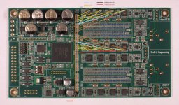
I have just discovered that the protocol I have published (coming from a quick view of the board without gears) is not correct, so I have to waste more time powering the board and analyzing data by the oscilloscope.
The voltage level shifting was obtained by AC coupling of all the signals coming from the FPGA followed by a resistor reference voltage for the 595s (positive or negative).
That's quick and cheap way but not what one expects from an absolute DAC.
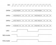
The dirty signals (BCK and DATA) share the ground of the crucial signal (Latch) for a R2R DAC.
... so it mostly depends of the phase noise of the output masterclock while there are between no and very slight dependance of the input masterclock.
It depends exclusively on the phase noise of the output masterclock, since the latch comes directly from the master clock and it's well isolated from the FPGA and the micro, so from the input.
And ours oscillators are really low phase noise, in the region of BVA and BT ULN.
You math lack however 🙂
//
N-Samples / SR >>> 4'000'000 / 44100 Hz = 90.7 seconds = 1.5 minutes

You are confusing the bit clock with the word clock.
Implementing a true FIFO buffer with low phase noise clock on the Soekris DAM1021 DAC
And the SRAM is in Mega bit not Mega byte.
Implementing a true FIFO buffer with low phase noise clock on the Soekris DAM1021 DAC
And the SRAM is in Mega bit not Mega byte.
Last edited:
It depends exclusively on the phase noise of the output masterclock
Ok, and why do we really needs FIFO reclock at the input while we can't remove intrinsic interpolating?
And ours oscillators are really low phase noise, in the region of BVA and BT ULN.
Heh, yes, i got one too.

There is no "intrinsic interpolating".
A fifo buffer is completely bit transparent. No processing is to be done whatsoever.
//
A fifo buffer is completely bit transparent. No processing is to be done whatsoever.
//
There is no "intrinsic interpolating".
Ok.
Let me know what do happen at the output inbetween the original I2S samples and why?
A fifo buffer is completely bit transparent. No processing is to be done whatsoever.
Have no doubt, i know first hand what FIFO is.
You are confusing the bit clock with the word clock.
Implementing a true FIFO buffer with low phase noise clock on the Soekris DAM1021 DAC
And the SRAM is in Mega bit not Mega byte.
Well, we deal hear with PCM and not DSD or I am wrong? While on PCM samples counts..
So at the end of the day we deal with samples given at LR-Clock at sample rate.
Also using samples, so we have to calculate 8M (bits) / 8 (bits/byte) / 4 (bytes per sample) 😱
We are talking about a 16 or 24 (32) bit word (sample!) system, yes. Whats so surprising?
44100 sample per second and channel (2) is red book CD.
//
44100 sample per second and channel (2) is red book CD.
//
Ok, and why do we really needs FIFO reclock at the input while we can't remove intrinsic interpolating?
Heh, yes, i got one too.
View attachment 904673
Sorry, I have not understood the question.
We need a FIFO buffer with a different clock just to isolate the DAC from the source.
So the source and the DAC operate in a different time domain and the quality of the source (jitter) will no longer matter.
Have no doubt, i know first hand what FIFO is.
I have some doubt... this fifo has memory - a lot.
//
Ok.
Let me know what do happen at the output inbetween the original I2S samples and why?
Have no doubt, i know first hand what FIFO is.
Me too I have not understood the question.
We need a FIFO buffer with a different clock just to isolate the DAC from the source.
So the source and the DAC operate in a different time domain and the quality of the source (jitter) will no longer matter.
It depends exclusively on the phase noise of the output masterclock, since the latch comes directly from the master clock and it's well isolated from the FPGA and the micro, so from the input.
Just reread both of those statements together.
- Home
- Source & Line
- Digital Line Level
- Implementing a true FIFO buffer with low phase noise clock on the Soekris DAM1021 DAC