Now put your board to corrode.
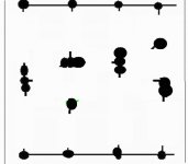
will result some dots and positive horizontal line (up) and negative horizontal line (down)..... and depending the circuit you may have other lines, as ground, feedback, input large dots and output large dots, thick lines were you have current... well...some details are up to you to deduce and to decide.
Now you have your board... clean it and melt a lot of solder over the lines..they will result thick and will resist to 20 amperes without melt... solder your parts direclty over the board, without produce holes....
The board back will be used to fix into chassis...you just use glue.
I will produce a video to youtube soon, about this amplifier, the Dunlap Amplifier, and you gonna see i am using other amplifier board.... every copper line can be used as a junction point.... when experienced, skilled with this method you can use any board into any schematic.
Of course this does not result pretty..but result easy and very fast.
Not more than 5 minutes to draw a board.... this is for real man..the ones does not bother if things are pretty.... real man wants things strong, fast, good to be made and that gives you free time to be running to catch your life.
The conventional, standard method uses a lot of time...so.... this is life time...not a good idea to waste for prototypes...only to make final units.
regards,
Carlos
Attachments
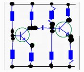
So... as you see...it is JUST the schematic placed
into the board, nothing can be more simple or easier.
Take some experience to decide distances...first you gonna need to watch part and to place them over the board to decide distances between dots...but this happens just the first time.
Second time you gonna do it easier and faster.
This is "Dx melting solder method"..unregistered and if you observe, it uses the SMD way to do things...i am proud i was the first to think about that.
regards,
Carlos
Attachments
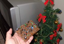
This was my first Roender amplifier board
I had not courage to dismount...his amplifier sounds nice.
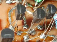
You see, the flux can be cleaned using Alcohol...or wiskie, Vodka..well... a lot of things dissolves flux.
Too much off topic....further conversations about come to my direct E mail adress:
panzertoo@yahoo.com
regards,
Carlos
I had not courage to dismount...his amplifier sounds nice.
You see, the flux can be cleaned using Alcohol...or wiskie, Vodka..well... a lot of things dissolves flux.
Too much off topic....further conversations about come to my direct E mail adress:
panzertoo@yahoo.com
regards,
Carlos
Attachments
Hello to all,
About the schematic of this modified diamond buffer. If you consider there is only around 2 diode voltage drops between the bases of the 2 "cascode" transistors, if you substract from it the 2 base-emitter voltage drops of the input transistors you are left with... lets say almost nothing. So the collector-emitter voltage drop for the "cascoding" devices is more or less only a diode voltage drop, so it's less than 1V, so these transistors are in saturation mode and should behave like (imperfect) resistors of small value in serie with a diode voltage drop. So in the end they are like a diode. Did I miss something, probably... Anyway... And how would it prevent the output to switch off in these conditions? I will put this in Micro-cap to investigate...
Thanx
Darian:
Did you do the sim on this circuit? I'm sure some of us would like to see the results. You should find find all the voltages are there in the proper amounts.
This is a polite way of saying your analysis of how the bias works is incorrect.
Steve
Did you do the sim on this circuit? I'm sure some of us would like to see the results. You should find find all the voltages are there in the proper amounts.
This is a polite way of saying your analysis of how the bias works is incorrect.
Steve
Carlos,
Did you build a fully working version of Steve's amp? How does it compare to your DX amps?
And again, a big thank you to Steve for sharing this circuit - much appreciated
Did you build a fully working version of Steve's amp? How does it compare to your DX amps?
And again, a big thank you to Steve for sharing this circuit - much appreciated
Dear Mr Dunlap
At first, thank you for your answer, at least your comment is telling me someone cares about my post in this thread, it's encouraging... I put your circuit under Microcap and it is very difficult to balance for a 0 DC output by itself. Well, with 10m in each arm, at idle, the upper "cascode" transistor has only 0.2V from emittor to collector and the lower has more, about 0.6, which is still quite in the "resistive" part of the diagram to me. These values don't vary much even in dynamic state with 40V of input swing. The 2 "bypass" diodes are off and they stay like that even with a 40V swing input (80uA is passing through the lowest one, it's low). The distortion is not low and is falling with the input level increasing, primary 3rd harmonic. So I'm still confused about it. Maybe the schematic is not accurate, I don't get it. Maybe you could be a little more explicative about how it is supposed to operate? Thank you for your help anyway. I am sure I missed something. This is a proven design so I should work. Still I don't get how you get these diodes to switch on with this schematic and with the 180 ohm bypass resistor!
Regards
Attachments
Sorry, for the lower transistor I mistyped, you should read 0.26V and 40uA for the diode. This is even more in the resistive part...
Regards
Regards
Re:
Carlos
I am very sorry to hear Graham is dead.
I know about death. I know about tears. I know about missing. I know about pain.
My best friend ever will be put into ground next friday.
We know all will die.
But when someone goes away, we have no defence, yet.
Does not matter if you prepare ....
When death comes close to you .... you will be hurt deeply hurt.
If you love your friend.
Lineup
Originally posted by destroyer X
Unfortunattelly we have lost Graham Maynard (not into the forum anymore)
Because we had one guy bothering him a lot inside this forum.
We have lost Graham...a big pitty..almost a crime against our community the one had bothered him.
Graham was a scientist... he told about EMF...he told about Standing waves and distortion...first cicle distortion..also he told about how to correct crossover distortions into class AB amplifiers.
Carlos
I am very sorry to hear Graham is dead.
I know about death. I know about tears. I know about missing. I know about pain.
My best friend ever will be put into ground next friday.
We know all will die.
But when someone goes away, we have no defence, yet.
Does not matter if you prepare ....
When death comes close to you .... you will be hurt deeply hurt.
If you love your friend.
Lineup
I am happy to tell you he is alive
And a moderator have informed he had activity into the Loudspeaker forum.... was lumanauw... and i think was in this thread.
He is not more contributing, writting into our forum, but i think he is alive.
Dead for this forum.... dead for the Solid State forum...absent is a more correct world.
Sorry, was my mistake, my confusion, my english, my error.
I am not absolutelly sure, but seems he is between us...in this same planet... and alive.
Graham is a hundred thousand miles ahead of many of us related know how... i think my ignorance may have bothered him a lot..also other folks ignorance... he is now researching about speakers.... the real solution is there.
regards,
Carlos
Darian.... not all folks have knowledge to understand your amplifier
So.... some of them have nothing to say.... how to comment something they do not understand.
Others know that deeply and feel your informations having nothing new to be commented.
Just that..sometimes we reach people and sometimes not.
For sure people cares one related the other..we are rarities in this world... crazy alike us exists less than 100 thousand folks around the world... each one of us are really important to the communitty.
Of course there are popular countries and less popular countries.... some folks from Planet Zeon 435 (for instance) if not very educated can "burn" some country image and this results in people not very interested into that special Zeon flag, because Zeon folks seems boring....not your case for sure.... this is only an analogie, and example to understanding.
C'est la vie...très problematique!
regards,
Carlos
Nice symmetrical amp, Carlos.
But really, in truth, I hope I never HAVE TO listen to that one 😉
The 7th order harmonic is crazsilly enouurmous ..
/halojoy
But really, in truth, I hope I never HAVE TO listen to that one 😉
The 7th order harmonic is crazsilly enouurmous ..
/halojoy
lineup,
It`s somewhat annoying in the beginning (the first twenty years) gradually getting easier.But really, in truth, I hope I never HAVE TO listen to that one The 7th order harmonic is crazsilly enouurmous ..
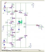
The schematic I posted is Mr Dunlap output,
Not mine! I think Dx and Lineup misunderstood, or I misunderstood their comments... This is the screencapture of Mr Dunlap output in Microcap since I really wanted to understand, and I couldn't get the low emittor to collector voltage of the "cascode" transistors. I agree, the distortion is almost purely odd harmonics and up to the 7th mainly.
Regards
darian.
i think, you must have drawn something wrong in that output stage
i just cant see how that circuit can work
i am sure when you can change and get it right
it will show a very good output stage
Regards
Lineup
i think, you must have drawn something wrong in that output stage
i just cant see how that circuit can work
i am sure when you can change and get it right
it will show a very good output stage
Regards
Lineup
Hey Lineup,
That's exactely what I am trying to understand, how it could work! Intuitively, for me it didn't, and on Microsim it didn't work either. That's why I am wondering if, there is not a mistake in the schematic. You can feel free to double-check on the original schematic if I didn't make mistakes. Mr Dunlap circuit is posted on post 114 earlier in the thread. I am just a very curious person so if everyone talks about a circuit for 8 pages and there is no real explaination about it, I get frustrated, that's what happened on this thread and that's why I try to simulate it because I know sometimes in electronic intuition is not enough... Someone on this forum taugt me that the hard (harsh) way...
Regards
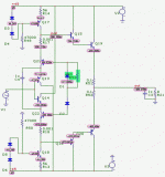
We see what Steve will say.
The part I can not understand, and what looks wrong to me.
is where Q13 and Q14 EMITTERS goes into Q21 and Q22 COLLECTORS.
This would normally not give a welldefined voltage.
Now, there may be some things I have still to learn to understand 😉
In a diamond EMITTERS connect to output BASES and so it works well.
- Status
- Not open for further replies.
- Home
- Amplifiers
- Solid State
- I have found a special amplifier, am trying to contact the designer