The minimum amplitude resolution of the amplifier output signal, assuming the output at its maximum elongation, is allowed by the power supply noise and the noise of the active and passive components reflected at the output.
If the power ripple is not taken into account, it is very likely that these minimum resolutions will be masked by the ripple itself (at least). I am not considering the amplifier's own noise or that of the voltage regulators themselves, which could be more determining.
Best regards
If the power ripple is not taken into account, it is very likely that these minimum resolutions will be masked by the ripple itself (at least). I am not considering the amplifier's own noise or that of the voltage regulators themselves, which could be more determining.
Best regards

I'll give an example, to quantify the filtering capacitor:
Let's assume an average power supply of 27 Vdc. For this power supply, it is expected to achieve a minimum of 17.95 Vpp at the output. If the reproduced signal has an amplitude resolution of 16 bits, the minimum valid output amplitude would be 65536 times smaller than those 17.95 Vpp. This gives approximately 274 uVpp, which is a probable value greater than the random noise of the amplifier (a value that would have to be checked in practice, since I have not measured it with REW).
Knowing that the PSRR of the amplifier at the home network frequency is approximately 78.16 dB, we could allow a ripple in the 27 Vdc line of 8093 times those 274 uV. That is, up to 2.22 Vpp, so as not to mask the minimum signal resolution by the power ripple (at least).
Applying a quick approximation with I = C x dV/dt, we can size the main filter capacitor. The peak current through the load will be (17.95 Vpp / 2) / 8 ohms = 1.12 A.
dt = 0.01 s for 100 Hz mains frequency (in reality, the time is somewhat shorter, but we are simplifying calculations). dt = 0.00833 s for 120 Hz.
dV = 2.22 Vpp stipulated above
Then, C = 5053 uF approx. (for 100 Hz), which due to tolerances of 20%, it is advisable to foresee about 6317 uF (6800 uF in practice).
For higher resolutions, the capacitor bank is multiplied by the resolution change rate (if the random noise of the amplifier allows it). This is x 16 or x 256 times, as the case may be. Since it is not economically viable, I suggest inserting regulators, as long as their random noises also allow it, which implies a much more complex analysis to do.
Best regards
Last edited:
No problem IAIMH!😊
Thank you for the thoughtful reply Diego, there is a lot to chew on here.
Most times I just use brute force with filter caps, Hahaha!!
Thank you for the thoughtful reply Diego, there is a lot to chew on here.
Most times I just use brute force with filter caps, Hahaha!!
@Vunce and @diegomj1973 -
The timing of this was uncanny. I was trying to determine what was going on with an amp I was measuring at the same time. Guess what?! PSU 'noise' / ripple was higher in amplitude that the harmonic distortion of the DUT (at a particular output). It took me quite some time to figure it out, but reading your exchange helped tremendously.

The timing of this was uncanny. I was trying to determine what was going on with an amp I was measuring at the same time. Guess what?! PSU 'noise' / ripple was higher in amplitude that the harmonic distortion of the DUT (at a particular output). It took me quite some time to figure it out, but reading your exchange helped tremendously.
If you try to keep everything simple, with a power ripple rejection of around 78 dB at frequencies of 100 to 120 Hz offered by this small amplifier, a basic scheme will be sufficient and effective: transformer, rectifier and main filter capacitor. The LM317 performs excellently well several jobs where I set it up in the circuit.
From the simplicity of the design it could be scaled to the extent that the hardware allows it and the capacitance multiplier is a possibility to use on that upward path, without losing sight of the limits imposed by the formats that we wish to reproduce along with those of our hardware.
Let's also not forget the modest parameters of the amplifier, factors that put less pressure on the power supply design.
In a very high-performance amplifier, the design of the power source takes on a totally different role, to the point of being as or more important than the amplifier itself, IMHO. I am not referring to esoteric things (a line of thought that I do not share), but only for noise and crosstalk issues, among the most important things.
Best regards
Last edited:


Electrical current flow in loops. Large loops act as antennae and may receive and broadcast noise. So keeping loop area small reduces the noise that may be emitted and picked up.
Here is the area within the loop of the DC flow within the power supply pcb:
Here is the area within the loop of the DC flow within the power supply pcb:
Attachments
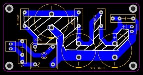
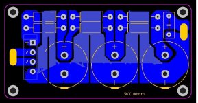
Here are two suggestions to reduce the loop area further. The second may be better. A third suggestion is to put a ground plane on the bottom side of the board. That may be the best.
By the way, an amplifier has several current loops and they all can be vulnerable to noise. There is the DC supply loop, the input signal loop, the speaker signal loop, etc.
By the way, an amplifier has several current loops and they all can be vulnerable to noise. There is the DC supply loop, the input signal loop, the speaker signal loop, etc.
Attachments


This modest power supply design could be used with acceptable results in the 27Vdc powered option, where R1 and R2 in the amplifier schematic are set at 1 ohm each.
Remember to provide a heatsink suitable for dissipating up to 15W for the voltage regulator of this same power supply.
The output voltage of the secondary winding of the power transformer should be between 25.7 Vac and 29.2 Vac. The suggested power should be between 80 to 120 VA per channel.
Best regards
There is room to squeeze out of the circuit, so I have made a simple table with which you can play according to your needs and tastes.

Best regards
Best regards
Great work Diego. My hat is off to you.
🙂
🙂
Quite the contrary, Nelson. You are my source of inspiration and your generosity is infinite.
The best for you. 🙂
The best for you. 🙂
- Home
- Amplifiers
- Pass Labs
- Hybrid ZEN Amplifier + LM317 = Efficient and simple