Hi,
every now and then, I´m thinking about HV amp topologies for ESL useage.
Here´s one that´s probabely been around for ages and I´m not sure yet if it is really feasable. So Your input is required 🙂
The aims are:
- just a single HV-supply
- push-pull for increased efficiency
- no global feedback, yet acceptably low THD
- scalable to different HV levels and ESL Loads
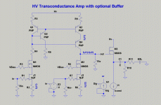
Anyway, attached is the principle schematics:
The circuit consists of a couple of subassemblies, such as:
a) 2pcs. of voltage to current converters
b) a current mirror
c) a current to voltage converter
d) a inverting amplifier stage
e) a Buffer
f) a ESL load
a) is made up from a low voltage N-channel JFET like the notorious 2SK170, BF862, 4391 et al.
The JFET is then cascoded by a HighVoltage N-channel enhancement MOSFET
Vbias may be as low as 10V to supply for the JFET a constant drain potential of as low as 6-8V. The bias is of preferably low value to allow for largest signal modulation amplitude.
The idle current through the JFET and as such through the whole cascoded branch is set by the source resistors R2 (resp. R8).
R4 is just a voltage dropper to decrease heat losse in MOSFET M1.
The second VI-converter is driven by a signal inverted to the input signal and scaled up to achieve symmetrical ac-current amplitudes through Q4, resp. M2.
b) is the current mirror made up basically from Q1 and Q2.
Q3 is a helper transistor that fixes Q1´s collector potential at 1xVbe below it´s Base potential. Q4 does the similar for Q2.
At least in theory and simulation may Q1 and Q2 then be of lowvoltage types regardless of the value of the Hv-supply.
Q4 must be a HV transistor though.
c) the IV-converter is a simple high-ohmic resistor
d) a invering amplifier stage is required to achieve symmetrical current swings in the upper and lower half of the output stage.
e) the Buffer could be a simple source follower loaded either by a constant current source or a (inverted) modulated current source.
f) ESL load is self explaining
Functioning:
The first VI-converter transforms the signal voltage into a ac-current, added a idle dc-current, say 5mA +-1mA [I(J1)].
This current is mirrored into Q4.
The second VI-converter J2/M2 [I(J2]] does the same in principle, but receives a inverted drive signal.
The difference currents (dc as well as ac, I(J1)-I(J2)) flow through the IV conversion resistor Riv.
Riv may be of high value of up to 100k. Even very low ac currents thus generate high ac-voltage swings.
The dc voltage potential at idle is best chosen at about Hv/2.
Say Hv is 500V and Riv=100k. Then a dc current of 2.5mA is required to flow through Riv to give a Vidle of 250V.
If the idle current through J1/M1/Q4 is 5mA, then the current through J2/M2 needs to be 2.5mA.
So the current setting source resistor R8 must be higher in value than R2 in the first VI-converter.
If now the input signal is just inverted, but not changed in amplitude, the ac current swing through J2 would be lower than in J1/Q4.
So the inverted signal must also be increased in amplitude by a factor X to achieve same current amplitudes, which is the point of highest efficiency.
The therefore required inverting amplifiying stage d) could be a simple single-transistor common-source or common-emitter stage.
Since the output impedance over Riv is close to Riv´s value a dedicated Buffer e) may supply for a high current capable, low impedance output.
Of course may the high impedance output be directly used to current-drive a ESL load.
In that case it might be a good idea to design the current mirror, such that a low current in the first branch is scaled up and mirrored into the second branch, by either reducing R9´s value or by using multiple R9/Q2 combos.
In any case does this topology allow for very high gains (>60dB ) with low THD, at good efficiency and without relying on global feedback.
The described and shown circuit represents just one half of a bridge circuit.
The complete circuit needs to be doubled, with the ESL load spanning between the two outputs.
Comments welcome 😉
jauu
Calvin
every now and then, I´m thinking about HV amp topologies for ESL useage.
Here´s one that´s probabely been around for ages and I´m not sure yet if it is really feasable. So Your input is required 🙂
The aims are:
- just a single HV-supply
- push-pull for increased efficiency
- no global feedback, yet acceptably low THD
- scalable to different HV levels and ESL Loads
Anyway, attached is the principle schematics:
The circuit consists of a couple of subassemblies, such as:
a) 2pcs. of voltage to current converters
b) a current mirror
c) a current to voltage converter
d) a inverting amplifier stage
e) a Buffer
f) a ESL load
a) is made up from a low voltage N-channel JFET like the notorious 2SK170, BF862, 4391 et al.
The JFET is then cascoded by a HighVoltage N-channel enhancement MOSFET
Vbias may be as low as 10V to supply for the JFET a constant drain potential of as low as 6-8V. The bias is of preferably low value to allow for largest signal modulation amplitude.
The idle current through the JFET and as such through the whole cascoded branch is set by the source resistors R2 (resp. R8).
R4 is just a voltage dropper to decrease heat losse in MOSFET M1.
The second VI-converter is driven by a signal inverted to the input signal and scaled up to achieve symmetrical ac-current amplitudes through Q4, resp. M2.
b) is the current mirror made up basically from Q1 and Q2.
Q3 is a helper transistor that fixes Q1´s collector potential at 1xVbe below it´s Base potential. Q4 does the similar for Q2.
At least in theory and simulation may Q1 and Q2 then be of lowvoltage types regardless of the value of the Hv-supply.
Q4 must be a HV transistor though.
c) the IV-converter is a simple high-ohmic resistor
d) a invering amplifier stage is required to achieve symmetrical current swings in the upper and lower half of the output stage.
e) the Buffer could be a simple source follower loaded either by a constant current source or a (inverted) modulated current source.
f) ESL load is self explaining
Functioning:
The first VI-converter transforms the signal voltage into a ac-current, added a idle dc-current, say 5mA +-1mA [I(J1)].
This current is mirrored into Q4.
The second VI-converter J2/M2 [I(J2]] does the same in principle, but receives a inverted drive signal.
The difference currents (dc as well as ac, I(J1)-I(J2)) flow through the IV conversion resistor Riv.
Riv may be of high value of up to 100k. Even very low ac currents thus generate high ac-voltage swings.
The dc voltage potential at idle is best chosen at about Hv/2.
Say Hv is 500V and Riv=100k. Then a dc current of 2.5mA is required to flow through Riv to give a Vidle of 250V.
If the idle current through J1/M1/Q4 is 5mA, then the current through J2/M2 needs to be 2.5mA.
So the current setting source resistor R8 must be higher in value than R2 in the first VI-converter.
If now the input signal is just inverted, but not changed in amplitude, the ac current swing through J2 would be lower than in J1/Q4.
So the inverted signal must also be increased in amplitude by a factor X to achieve same current amplitudes, which is the point of highest efficiency.
The therefore required inverting amplifiying stage d) could be a simple single-transistor common-source or common-emitter stage.
Since the output impedance over Riv is close to Riv´s value a dedicated Buffer e) may supply for a high current capable, low impedance output.
Of course may the high impedance output be directly used to current-drive a ESL load.
In that case it might be a good idea to design the current mirror, such that a low current in the first branch is scaled up and mirrored into the second branch, by either reducing R9´s value or by using multiple R9/Q2 combos.
In any case does this topology allow for very high gains (>60dB ) with low THD, at good efficiency and without relying on global feedback.
The described and shown circuit represents just one half of a bridge circuit.
The complete circuit needs to be doubled, with the ESL load spanning between the two outputs.
Comments welcome 😉
jauu
Calvin
Attachments
What happens when you have two current sources hooked in series, one fed from ground and the other fed from supply and the currents are not quite the same?
Answer: The Voltage will go towards the higher current source...not near the midpoint.
This looks like what might happen.
Correct me if this is not the case.
🙂
Answer: The Voltage will go towards the higher current source...not near the midpoint.
This looks like what might happen.
Correct me if this is not the case.
🙂
first of all, there are no pnp devices that will handle several kV, so Q4 is unobtanium... No p-channel mosfets for this kind of voltages exist either. That is in fact the major issue with direct drive designs: you can't built a proper push pull design using only one polarity of devices.
Second, use of current mirrors imply the introduction of points of very high impedance in the circuit. Stray capacitances will be coupling all kinds of signals into those points that you do no want. Especially in a design were signals of several kV are happily swinging around all over the circuit this is something to take very seriously (I can speak from experience). I doubt it will be possible to get it to work at all without oscillating.
Third,
If it was easy it would have been done a long time ago 😉
Second, use of current mirrors imply the introduction of points of very high impedance in the circuit. Stray capacitances will be coupling all kinds of signals into those points that you do no want. Especially in a design were signals of several kV are happily swinging around all over the circuit this is something to take very seriously (I can speak from experience). I doubt it will be possible to get it to work at all without oscillating.
Third,
That buffer stage is not optional but badly needed, you need approx 25mA current capability per kV of swing to drive a full range esl so we're looking at 200mA pp for a design running from 4kV rails. A source follower with a ccs will not do, dissipation will be too huge to be practical. A modulated cs would help but how do you want to get it to work decently. Stacking 2 current sources will never work decently as a linear amplifier, as dug already stated. You will need lots of feedback.e) the Buffer could be a simple source follower loaded either by a constant current source or a (inverted) modulated current source.
If it was easy it would have been done a long time ago 😉
Last edited:
Hi,
Regarding the two current sources, have You missed the role of Riv?
Without Riv You´d be right, in that the voltage level would be undefined
Any difference between the two current sources is routed through Riv.
This gives a defined voltage level of (I1-I2)*Riv.
I see no reason why this should apply to complementary transconductance stages with split supplies (AD844, OPA860, etc.) only, but not to a singleended singlesupply circuit? 😕
The danger of oscillation has to be kept in mind, I agree fully with that.
Also a Yes to the problems of sourcing useable P-devices for Q4.
There are just very few P-channel MOSFets with <-500V Vds.
Fairchild offers some candidates like the FQB1P50 Which is intersting due to its low capacitances.
This restricts the circuit probabely to rather lower voltage ranges of <1kV even if we cascode Q4 😡 But for a HP it could suffice.
A turnaround at least for the first VI-converter stage could be to change to a complementary circuit with J1=P-JFET, M1=P-MOS, cascoding M1 with P-MOS, Q1-Q3=NPNs and Q4 a HV-N-channel MOS, and negative supplies.
As there´s no considerable voltage swing, simple constant voltage biasing the Gates would suffice for the cascode devices.
The second VI-converter would still face the problem, that the cascode devices would need a sliding bias voltage, referenced towards the output voltage.
Maybe one should replace the second VI-converter then by a simple Load resistor connected against gnd and omit with pushpull drive.
At least should there be enough drive capabilty to feed a Buffer input.
Large Panels would require the Buffer anyway, yes. Although this means to sacrifice on current drive and to apply voltage drive again.
Seems we need a
jauu
Calvin
Last edited:
Hi,
Regarding the two current sources, have You missed the role of Riv?
Without Riv You´d be right, in that the voltage level would be undefined
Any difference between the two current sources is routed through Riv.
This gives a defined voltage level of (I1-I2)*Riv.
...
If I2 > I1 then V=0
Thermal stability of J1 vs J2 is another question even it you could balance the current sources with an adjustment.
If you had one fixed and the other was supplied with DC feedback it would work. (as far as a stable DC output goes)
Seems we need a
no need for miracles, a decent low capacitance 1kV P-channel mosfet is all we need 😉
"no need for miracles, a decent low capacitance 1kV P-channel mosfet is all we need "
Ahhhh,ha,ha,ha,ha...That would be a miracle as the only P-channel Mosfet the any one is making right now are under 100v or so!! 😉
I have finally got a bunch of HVfet's and I too have been seriously thinking about using them and getting the idea of DD amps for ESL's off of the drawing board and into reality.
Just in case you have not seen this thread here is a very interesting project as well,
http://www.diyaudio.com/forums/pass...-headphone-amplifier-concept.html#post3753546
I am with you on this one Calvin, I will take a closer look at your design.
I also do like the use of opamp's as well as it seems to simplify the design and worked very well for my First prototype at only 200v.
Carry on, just my 2 cent's FWIW.
jer 🙂
Why don't you use tube amplification?....they are a high voltage swing source...before they get to the output transformers????? How much do you wanting to swing & how many mA load?
__________________________________________________Rick......
__________________________________________________Rick......
Vt's are much more Expensive!!
I have two 833's and one has lost its vacuum and I haven't even used them yet.
A few years ago you could get one for about $30 but that is definitely the case now.
FET's are much cheaper and I'll bet more linear too.
It only takes a few Volts to drive a HVFET unlike a good ole' VT such as the 833.
It takes at least 2Kv of swing to get good sound out of an ESL panel depending on its size and the current it requires is analog to Ohms Law depending on its capacitance.
Even though a good listening level may only be around 500v or so this doesn't leave any room for +10db transient pulses commonly found in music samples.
STmicroelectronics is now making 1700V fet's with a power rating in the 300 to 400 watt range for just a few Dollars!!!
This is much much better than the price of a hard to find VT !! 😉
jer 🙂
tubes also happen to come in one polarity only. Something with physics and electrons and so 😀 So tubes offer no solution here either.
It all boils down to: how to make a decent linear push-pull stage running at 4kV with only one polarity devices. I summed it up a long time ago in this topic:
http://www.diyaudio.com/forums/planars-exotics/80714-another-direct-drive-thread.html
It all boils down to: how to make a decent linear push-pull stage running at 4kV with only one polarity devices. I summed it up a long time ago in this topic:
http://www.diyaudio.com/forums/planars-exotics/80714-another-direct-drive-thread.html
Hi,
I´d like to keep the thread to the discussion of Transconductance amps and preferrably to those featuring solid state devices.
Based on P.Walker´s suggestion to use current drive to an ESL Panel (Pat: US 3,773,984, Nov.1973).
The Patent suggests a series sense resistor on the transformer´s secondary to create the current drive.
To omit with the transformer onne needs an Amplifier with a high-impedance current output, either Transconductance or Transimpedance.
Hence this thread´s theme. 😉
I found out where I got idea with the current mirror from.
Matthew A. Schaning and Kurt A. Kaczmarek presented a complete description in "A High-Voltage Transconductance Amplifier for Electrotactile Stimulation".
Published as: IEEE Trans Biomed Eng. 2008 October.
See: A High-Voltage Transconductance Amplifier for Electrotactile Stimulation.
Interesting PNPs could be:
2SA1968 (-900V), PZTA96ST1G, MJE/MJD/KSE350, BSP16, DZTA92, FZT558, FZT758
P-Channel MOS:
BSP317P, BSP92P, FQD2P40, FQB1P50, IRFR/U9310, IXTH10P60 (-600V), VP0550, VP2450.
Attached is a Sim-File of a amp after #1.
included some subckt data.
Unfortunately I couldn´t get the IRFRU9310, the FQP2P40 and FQB1P50 subckts running. Maybe someone could solve this Prob?
I used the IRFP9240 data instead for M3/M6.
In the Sim a 70mVp (50mVrms) Input signal generates a Output signal of 13.3mApp through C2, translating up to 1.5kVpp (540Vrms) at THD<1%.
Wouldnt be to bad for a single-gainstage, non-feedback circuit.
jauu
Calvinn
Attachments
I see your point, however voltage drive is a nice theory but in practice it does not work. Based on that idea I once built a direct drive current amp, that had current feedback so it gave flat response in the current domain. It resulted in a frequency response that dropped considerably at higher frequencies. To put it simple: sounded like listening to a subwoofer. I added the schematic for reference.
The reason? Current driving an ESL give a straight response in the far field only. When you listen to an esl in near field it has to be voltage driven to give flat response (headphones!). In practice we listen to our esl's somewhere in between near- and far field.
In addition, the theory is valid only for an unsegmented esl. In most cases we have to use segmentation to get good dispersion and that will cause a dropping response at higher frequencies (less area).
So using pure current drive in a practical setup will not work, you need a mix of voltage- and current drive that in practice comes down to virtually only voltage drive.
With a design limited to 1kV or so I see little advantage in using this complicated setup. A simple ccs loaded SE design with 2 mosfets will do the same and by configuring your feedback you can choose between any mix of current and voltage drive.
Oh and keep in mind the SOA limitations and very low linearity and beta's of HV BJT's. You may be better of sticking to mosfets 😀
Attachments
I agree with others above that high voltage PNP or N-channel devices are unavailable. However it's fairly straighforward to design a push-pull class A output stage using only N-channel devices, with an SRPP topology. This will naturally give a high output impedance i.e. current drive, but the output impedance can be lowered, if desired, with feedback.
Yes, in fact nothing new under the sun. Acoustat used a srpp design ages ago.
The issue with srpp is that it will at best double output current over idle current. So it will at best result in half the dissipation compared to ccs. That is, in a perfectly matched resistive load. In a complex capacitive load such as a segmented esl it will not work very well, you will not get even near the benefits of halving dissipation. So basically it's just a slightly beefed up class A design.
In other words: by far not sufficient to built an amplifier with reasonable dissipation that will match up with the output of a simple esl transformer and that will drive a full range panel.
"srpp derived" modulated ccs with SS device with no triode tube design mu term looks like "impedance multiplier" that presents 1/2 the load
you really can't expect more - its the best that can be done in Class A
so you still have to drive C - just looks like 1/2 the value
for conventional audio frequency range step up xfmr are "impedance dividers" - with bigger ratio possible so your amps sees a much bigger C load
the real world xfmr parasitic esl, esr can give resonance just an octave above audio
Hi,
All my experiments ended with one single working prototype DD amp(class A with current source and IRFBG20s). The reason was that I started to measure distortion caused by step-ups. To my surprise the effect was not big, on par with amplifier and sound card, and in general up to an order of magnitude lower than non-linearity of ESL panel itself.
Conclusion : DD amp - difficult to build, dangerous, expensive for electricity(class A), might be even less linear than a good amp+trafo, so what for all the effort?
Regards,
Lukas.
Calvin,
the currents levels in amplifier seems to be almost an order of magnitude lower than it should be for the capacitances expected for SWITCH mode mosfets. Moreover newer trench ones have really non-linear capacitances which are NOT simulated properly in PSpice.
There is no demand for low power lateral mosfets - no go this way - no such things exist.
I would use CCS loaded cascode WITHOUT complementary devices. The only alternative could be low power rf HV tubes with real low capacitances. Anyway it's up to you to decide what level of hassle worth the performance.
Newly appeared SIC jfets again are tailored for high current/low on resistance - no small devices as well...
Bjt's seems to be better... with lower capacitances and higher trans conductances.
EDIT:
http://www.infineon.com/dgdl/Bsp300...c1f67&fileId=db3a30433b47825b013b4c980bd0110d
http://ixapps.ixys.com/DataSheet/DS100182A(IXTY-TA-TP08N100D2).pdf
http://ixapps.ixys.com/DataSheet/DS98809C(IXTP-U-Y01N100D).pdf
Last edited:
Maybe a selenium-diode amplifier inspired by the Lundahl Magamp or the David Berning ZOTL?
Last edited:
There is nothing wrong with thermoionic devices. Just ask high power RF equipment manufacturers or particle accelerator designers. Neither steam locomotives or selenium rectifiers are intrinsically bad. They all do work within the specs. Moreover absence of complementary (P-type) devices moves us into tube topology area.
- Status
- Not open for further replies.
- Home
- Loudspeakers
- Planars & Exotics
- HV Transconductance Amp - Idea