Hi Pierre,
The Feedback could be very easily referenced to Midpoint by using a level shifter at the output of SG3524 , GND reference the IC and then Level shift its output to -Vrail and connect it to the input of IR2111 and drive the mosfets and then take the feedback and apply it to the inverting pin of error amp of PWM IC.....
regards,
K a n w a r
Thanks, Kanwar, but I think that was clear from the start (that's what I did in my amp in fact, although with double level-shifter and a IR2113 chip 😀)
What I was trying to figure out is how to simplify it to the extreme by referencing the modulator chip to -Vrail, so no level shifter is needed, but then you have to AC couple the input signal, and feedback cannot be connected directly unless you AC couple it, producing DC offset error problems.
Anyway, I think that's a dead-end, because in the best of cases, you may need some kind of level-shift in the feedback signal, voiding the advantage of simplicity we were pursuing.
IMHO we could keep on defining an sch based on SG3524, as Kanwar's amp. However, for the sake of simplicity, I would like to work a little bit more on the concept of discrete driving instead of using a IR chip. I proposed a partial schematic and we are waiting for suggestions, critics or improvements.
Best regards,
Pierre
Hi, Pierre,
I really wanted to help with reviewing your idea of level shifter, but since I'm not familiar with classD design, nor I have other schematic to compare (the only SG3524 schematic that I have is on the first post, the defected one), I cannot help much here.
Maybe Kanwar can help with showing what he does with lo-fi SG3524 based classD? How about it, Kanwar? I think your commercial business wont be disturbed by showing this lo-fi design of yours. But it can teach us something 😉
I have detected an error in the sch I posted. The second level shifter collector resistor (R2) should go to the bootstrap voltage, not to +12V.
Anyway, I will try to draw an sch of my amplifier, removing my PWM modulator and exchanging it for a SG3524. That's pretty close to what Kanwar suggests.
Best regards,
Pierre
Anyway, I will try to draw an sch of my amplifier, removing my PWM modulator and exchanging it for a SG3524. That's pretty close to what Kanwar suggests.
Best regards,
Pierre
Yes, I think it can be done.
I use a discrete modulator with input stage, triangle generator, comparator, etc, but everything is in the SG3524 (although you won't get the same level of performance ;-)
I use a discrete modulator with input stage, triangle generator, comparator, etc, but everything is in the SG3524 (although you won't get the same level of performance ;-)
Hi, Pierre,
Looking forward for the sch 🙂
It seems the Triangle generator is more like Sawtooth generator, is it a problem?
Looking forward for the sch 🙂
It seems the Triangle generator is more like Sawtooth generator, is it a problem?
It shouldn't be a problem with the sawtooth generator. With the outputs wired in OR configuration, you still get 0 to around 90% duty-cycle.
I will try to draw it today so I can show it to you at the end of the day and comments can be received.
Only a detail: presumably, soft-start of the modulator should occur before the output drivers are activated, as 0% duty cycle will correspond to near -Vrail output. It should be stablished at 50% before output starts switching.
Best regards.
lumanauw said:
Maybe Kanwar can help with showing what he does with lo-fi SG3524 based classD? How about it, Kanwar? I think your commercial business wont be disturbed by showing this lo-fi design of yours. But it can teach us something 😉
Hi David,
There's no problem on the schematics, but i have to draw it , then i would be able to post it......thats not my commercial project, I would certainly like to share it with you guys... 😉
K a n w a r
Is the high side gate driver of the first circuit useable? I saw some ringing in simulation of something like this.
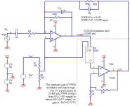
Here is a proposal of a Class-D amp based on a SG3525 and IR mosfet driver chip, with only a level shifter.
The circuit is only a proposal and must be reviewed and perfectionated.
Some hints...
- SG3525 is very similar to SG3524. I am more used to it, but SG3524 has open collector output stages that make the diodes unnecessary.
- Switching freq. is around 80KHz here, but can be modified by means of CT1 and RT1.
- There is only a level shifting, it produces an inverted version of the PWM, that hence must attack directly to the low side driver input. The inverted version can attack the high side driver input.
- Using this chip this way doesn't provide shutdown. To implement it, either use an IC that provides it, or simply add an AND gate before each input, so the shutdown signal enters both gates in order to make both inputs 0 simultaneously when it is "0".
- Dead-time is only taken care of at the mosfet gates. For more controlled dead-time, either use a chip with dead-time control (such as LM5104, but that doesn't have SD), or implement dead-time with a RCD circuit before each input.
- The input arrangement must be reviewed. I have biased the +IN to Vref/2, and AC coupled the input, but I don't know if that's totally ok.
- Compensation is not added. Perhaps it needs to be done.
- I haven't added the necessary supply bypassing caps near the mosfets. Those are taken for granted!
I hope this provides a good point to start working on for a mid-fi and very low cost Class-D amplifier, at least for subwoofer use.
Best regards,
Pierre
Attachments
Hi, Pierre,
Very nice, thank you 😀
SG3525 has totem pole output inherent in the chip, compared to SG3524, is this contributing something that makes you choose SG3525?
It consist only of 3 vital components (or 4, +4049 IC), that's good for this project 😀
To make it even simpler, maybe we can use IR2111, low cost, and can omit the 4049 IC? I can buy IR2111 here, quite cheap. For others, I should import it, making them will be expensive.
Oh yes, Pierre. I always wonder how to make classD a full bridge (like HIP4080 based). It won't have rail pumping due to heavy subwoofer work (when headed to half bridge topology).
Is it possible to make this lo-fi, lo-cost, SG3524 based classD a full bridge one?
Another one. How to calculate the compensation(s) / feedback networking for any classD? Does it needs Simulator, or can be done with calculator?
IR2111 can be ok, but it is quite slow (only about 400mA drive) and it doesn't have SD nor dead-time control. You really need shutdown in order to control start-up and add protections such as overcurrent.
I have chosen SG3525 only because I had the symbol created for Protel ;-) You can freely use SG3524 and that should be ok too. Connection is very similar.
About full-bridge: Yes, it can be done very easily. You only need two mosfet drivers (one for each "side"), but with the inputs inverted. The filter changes, too, and so does the feedback.
IMHO, it is better and easier to build two half-bridge amps and then connect them in bridge-mode. The only added component is another SG3524/5 and an opamp for signal inversion to one of them.
About feedback, if you use this for subwoofer where ultra-low distortion and frequency response doesn't need to be load independent, feedback can be taken before filter (ZAP pulse does that, for example), and compensation is very easy or perhaps simply solved by adding a cap between inverting input and COMP terminal, as shown.
That needs experimentation, however.
Hope you get the time to build one and tell us how it works!
I have been doing some tests with SG3524 trying to generate a 0% to 90% PWM. If I haven't done something wrong, the arrangement shown in the initial figure posted by lumanauw (both output transistors inside the chip connected in parallel, with emitters to GND and collectors with a pullup to Vcc, output at collectors), won't work: as both outputs won't never be active at the same time, at any moment one of the transistors is saturated and pulling down, so output will be always 0V.
I think the correct arrangement for OR configuration (output is high whenever one of the outputs is high), transistors must still be connected in parallel, but collectors must go to VCC, and emitters to output, with a 620ohm or so pulldown to GND.
It still remains to see if this arrangement inverts, in which case polarity of the PWM should be inverted (i.e, output of the level shifter should go to HS driver and after inverting it, to LS driver).
Just some ideas...
Pierre said:I have been doing some tests with SG3524 trying to generate a 0% to 90% PWM. If I haven't done something wrong, the arrangement shown in the initial figure posted by lumanauw (both output transistors inside the chip connected in parallel, with emitters to GND and collectors with a pullup to Vcc, output at collectors), won't work: as both outputs won't never be active at the same time, at any moment one of the transistors is saturated and pulling down, so output will be always 0V.
I think the correct arrangement for OR configuration (output is high whenever one of the outputs is high), transistors must still be connected in parallel, but collectors must go to VCC, and emitters to output, with a 620ohm or so pulldown to GND.
It still remains to see if this arrangement inverts, in which case polarity of the PWM should be inverted (i.e, output of the level shifter should go to HS driver and after inverting it, to LS driver).
Just some ideas...
Oh Pierre,
I am afraid, you are wrong buddy, whether you take outputs from collector or from emitters the only difference is phase inversion...
K a n w a r
Apart from the signal inversion (which is only a minor problem BTW) connecting the collectors is a more elegant solution than connecting the emitters. Such an arrangement is called a "wired OR" by the digital guys BTW.
Regards
Charles
Regards
Charles
Kanwar,
I suppose you are right, because I have also seen that arrangement (connecting the emitters to GND and the collectors together produce the output with a pullup to VCC), but the thing is that I must be missing something, because when one of the outputs goes low, its transistor is activated, pulling the signal down to 0, so theoretically (I repeat, I must be wrong), output should be always 0, as both outputs are never 1 at the same time ¿¿¿???
Anyway. I have tried with the output taken from the emitters and it seems to work well (0 to 93% at 125 KHz).
I have also started a simulation in order to understand feedback and biasing better. In the schematics shown below, the first opamp is SG3524 internal error-amp. The other simulates the gain of the modulator and power stage.
Note that SG3524 produces 93% PWM when COMP is at around 3.5V, and 0% when it is below, say, 0.6V. So I have arranged the rest so that I can simulate that behaviour and get positive and negative output. Of course I have used any opamp I have found (TL082 can't be fed at +/-60V !!!) only to get the behavior.
The simulation works nice, you get the expected gain (RFB/R4) but there is always an offset that is only removed if I add a capacitor in series with the feedback resistor, that I don't like (it will produce DC droop, error, etc).
There must be a way to DC couple the feedback signal in unipolar-fed error amplifiers. Any ideas?
Attachments
Yes, it can be possible to build a full-bridge with a single SG3524, but you will need an additional opamp for the differential feedback, and it can become much more difficult.
I would recommend that you started with a half-bridge and then connect two of them in bridge mode.
I posted an sch that is being commented right now, when it is more clear and definitive you can start experimenting.
About the IR2111 driver, be prepared to have quite high switching losses, due to its small drive capability that will lead to slow rise/fall times unless you use small or low-capacitance mosfets. IRF640N is a good start. The only advantage of that chip is simplicity.
Be prepared also for turn on/off transients due to the lack of SD pin.
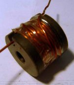
The coil is a drum core, isn't it? I started also with one of them from Wilco, with good results, although a iron-powder toroid core is better.
It only rests to fix the input/feedback coupling to remove the offset. The rest is quite straightforward, at least for a prototype.
Kanwar, can we have a look at your sch also?
I would recommend that you started with a half-bridge and then connect two of them in bridge mode.
I posted an sch that is being commented right now, when it is more clear and definitive you can start experimenting.
About the IR2111 driver, be prepared to have quite high switching losses, due to its small drive capability that will lead to slow rise/fall times unless you use small or low-capacitance mosfets. IRF640N is a good start. The only advantage of that chip is simplicity.
Be prepared also for turn on/off transients due to the lack of SD pin.
The coil is a drum core, isn't it? I started also with one of them from Wilco, with good results, although a iron-powder toroid core is better.
It only rests to fix the input/feedback coupling to remove the offset. The rest is quite straightforward, at least for a prototype.
Kanwar, can we have a look at your sch also?
- Status
- Not open for further replies.
- Home
- Amplifiers
- Class D
- How to fix this sch?