Greetings,
I have an Holfi integra amplifier, ver.1.1, I bought it thinking it would be an easy fix, but I didn´t expect to find every transistor on the power amp circuit replaced.
Can´t find any documentation online, I drawn a schematic to help me repair it. The output transistors were shorted so I replaced them, still it had full DC on the ouput, then noticed the first transistor (T1) was a 2sc2240GR and it needed more gain to get the proper bias, so I got a 2sc2240BL and solved the problem.
Now the only problem I have is no bias current on the output transistors and I find it weird to see a darlington BC879 as vbe multiplier (T6) that measures as a PNP instead of a NPN, and the pinout doesn´t seem to match the circuit board.
Does anyone know which is the original transistor? Is it viable to replace the base resistors and the transistor to a single npn instead?
Thanks.
Attachments

The connection of the T6 transistor is incorrect.Collector must be connect to 1, base connect to 2
I have seen MPSA13 used in the position of T6 in another Holfi amplifier. Also being an darlington transistor.
Mogens
Mogens
I have seen MPSA13 used in the position of T6 in another Holfi amplifier. Also being an darlington transistor.
Mogens
I already got it working with a new BC879, but MPSA13 seems to be the one. I will replace it.
Thanks for the help.
Hi
I have fairly the same problem, but with a version 1.3. There where different transistors on l an r channel…
It is not the exactly same schematic as shinobot2 and transistors changed (what looked original) now to:
2sa1302 / 2sc3281
SA1220 / SC2690
MPSA13
3 x SA970BL
1 x C2240BL
Does anybody know if this is right?
Powering up with vari-trafo at 120v left channel seems god, but right channel bias seems to get to high...…
DC ofset (TP1 and TP2) both channels is at 10v which is way too high, but could that be because the relay is not activated, due to the low power supply?
Hi baek47,
The output seems to be consistent with the NB3 I have. However, my input uses 3 x 2SC2440 and 1 x 2SA970.
Have you drawn the schematic or are you able to take some good pictures of bot sides of the PCB so we could draw the schematic?
The output seems to be consistent with the NB3 I have. However, my input uses 3 x 2SC2440 and 1 x 2SA970.
Have you drawn the schematic or are you able to take some good pictures of bot sides of the PCB so we could draw the schematic?
Holfi Integra 8
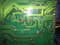
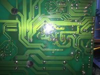
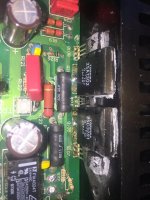
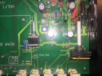
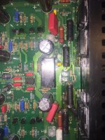
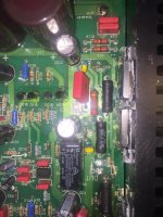
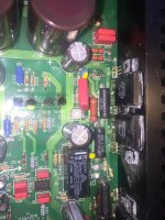
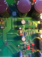
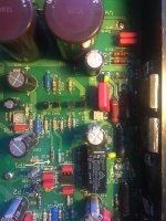
Hi....there are picture of left left channel.
Q108 is SA1220 - changed to new
Q110 is SA1302 - changed to new
Q111 is MPSA13 - changed to new
Q109 is 2SC3281 - changed to new
Q107 is SC2690 - - changed to new
Q101 is C2240BL - old, but probably not original
Q102, Q103, Q104 are SA970BL - old, but probably not original
I tried draw schematic, but I´m not skilled for that….
Let me know if its possible or to hard.
Lot of previous burns on right channel, but all cupper traces are good and tested for continuety….
Best from baek47
Last edited:
pictures
Attachments
-
 IMG_0593.jpg152.9 KB · Views: 337
 -
 IMG_0588.jpg175.3 KB · Views: 337
 -
 IMG_0589.jpg178.5 KB · Views: 386
 -
 IMG_0581.jpg124.8 KB · Views: 385
 -
 IMG_0580.jpg178.8 KB · Views: 375
 -
 IMG_0577.jpg154.5 KB · Views: 369
 -
 IMG_0575.jpg146.6 KB · Views: 708
 -
 IMG_0574.jpg149.7 KB · Views: 716
 -
 IMG_0572.jpg119.7 KB · Views: 744
 -
 IMG_0571.jpg128.9 KB · Views: 776
Hi baek47,
I have had a look at the pictures. Although it’s hard to see the resistor values I think I have a rough sketch of the schematic. I will try to start drawing it.
Just to make sure. You write you have to high a bias current in the right channel? Have you tried to power it full up to 230V?
I have had a look at the pictures. Although it’s hard to see the resistor values I think I have a rough sketch of the schematic. I will try to start drawing it.
Just to make sure. You write you have to high a bias current in the right channel? Have you tried to power it full up to 230V?
Hi mkc
Great, I can probably fill in the resistor values….
No I have only powered to ca. 120V (I am the cautius type). Nothing went hot at all and values left and right where the same until suddenly right channel changed from ca. 16v at TP4 to 9v/7,4v with 1,6v voltagedrop across TP4 resistor. Left side was at that point 16 mV. I did guess it should be around 20 mV running and adjusted...
Last edited:
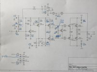
Hi baek47,
Here is first attempt on the schematic from what I could see in pictures. There is likely an error so please try to validate that I have got it right. Also, there are some component values missing so perhaps you can fill these in and I will add them.
integra_rev_01.pdf - Google Drive
Mogens
Here is first attempt on the schematic from what I could see in pictures. There is likely an error so please try to validate that I have got it right. Also, there are some component values missing so perhaps you can fill these in and I will add them.
integra_rev_01.pdf - Google Drive
Mogens
Hi Mogens. That is so so cool, thanks :- )
I check with boards and fill in missing values.
Thanks
Torben
I check with boards and fill in missing values.
Thanks
Torben
Hi Torben,
Great. It would surprise me if I hadn't made any mistakes. There are a few things that looks strange to me. The connection of R118 as an example. But, as far as I can determine it looks to be connected this way.
If there is interest we could document the whole amplifier.
Mogens
Great. It would surprise me if I hadn't made any mistakes. There are a few things that looks strange to me. The connection of R118 as an example. But, as far as I can determine it looks to be connected this way.
If there is interest we could document the whole amplifier.
Mogens
Hi Mogens
I have checked diagram with the amplifier - and I filled in missing values.¨
Yes - I think there are a few mistakes, but Im still more than impressed that you could go that far.….I have tried to check, with limited knowlegde on solid state amplifier, step by step....I think:
R118 is correct
TR3 is on one side connected to R122 and on the other side to R125, collector of MPSA13 and collector of Q103. Sounds right?
The R114m 116 and 117 should be swapped.
The pinnumbers on transistor doesnt match, but the symbols are correct.
I have put it in the schematic, see attached….and its a Holfi Integra 8 vers. 1.3
And then to the real embarresment, the elephant in my eye, the forest i couldnt see because of all the trees…aaaargh
I have replaced the to resistors on R05 and R06 on right channel - they were very burned...and not looking enough on the ones on left channel I bought and replaced R22 with 22R!!!! No wonder the bias was off……
No excuse for me, but I would never never have found the mistake without the schematic…...and im still in learning phase, I hope Im excused.
I havent tried with R22 but will asap - and thanks for helping me out.
I think it could be nice - also to others too, to finish the schematic. Ill try too draw it by hand and send it to you?
First Ill get some R22 and test again.
Does anybody know the values for testpoint T1, an T3? DC / bias..
Regards Torben
Attachments
Hi baek47,
Great it was of some benefit to you. If I had to mention all the stupid mistakes I made (Hey, I'm a software guy) it would go on. We just have to acknowledge and move on.
I'm ready for documenting the whole amplifier. I will update with your latest additions.
Mogens
Great it was of some benefit to you. If I had to mention all the stupid mistakes I made (Hey, I'm a software guy) it would go on. We just have to acknowledge and move on.
I'm ready for documenting the whole amplifier. I will update with your latest additions.
Mogens
- Home
- Amplifiers
- Solid State
- Holfi Integra