Why /how does this strange-looking stage work?
Well, this question is actually answered by the fact that it is self-explanatory. You /we just shouldn't necessarily stick slavishly to the idea of an LTP (classic differential amplifier with two bipolar transistors).
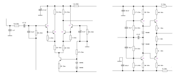
The chain consists of:
Idlecurrent is appox (and measured) 30mA_dc+ & 35mA_dc- !
HBt.
(currents are impressed)
Well, this question is actually answered by the fact that it is self-explanatory. You /we just shouldn't necessarily stick slavishly to the idea of an LTP (classic differential amplifier with two bipolar transistors).
The chain consists of:
- Q6 as an impedance converter (collector circuit), at whose emitter electrode the signal is decoupled and fed to the next stage
- Q5 as the coupling stage in base circuit (whose base electrode is the actual low-impedance input of the VAS)
- followed by Q3 & Q4 working in push-pull, voltage-amplifying emitter circuit (with high-impedance output resistor)
- and low impedance decoupled via Q1 & Q2 as push-pull emitter follower.
Idlecurrent is appox (and measured) 30mA_dc+ & 35mA_dc- !
HBt.
(currents are impressed)
Attachments
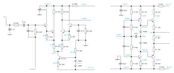
So Q3 and Q4 are the actual VA stage and not Q5,6,7,8. Q5 is actually only one possible form of coupling, unfortunately this is not entirely true, it does make a small contribution to amplification. However, we could now restructure the IP stage and no longer (only) consider it as a differential amplifier LTP -> simplify.
#
It is also a strange matter with the imaginary worlds, because Q5's collector also works at an apparent zero point, two static potentials of 0V each were electrically (galvanically) connected to each other. The measured potential is +285mVdc. It is therefore better to abandon the idea that measurable electrical voltages need to be amplified. We should look at currents, i.e. look inside the line /wire.
Last edited:
No. Everything is very clear.It is also a strange matter with the imaginary worlds, because Q5's collector also works at an apparent zero point,
Q5's collector just works at the voltage that the circuit demands. In this special arrangement, the VAS input is at ca. 0V, so to avoid output offset, Q5's collector must be at the same voltage.
(That voltage is determined by the ltp leg resistor and the total current including any VAS base and divider currents, so the resistor value has to be adjusted accordingly.)
Now you are left with a small Vce, that´s why I said "shallow water" in an early post.
But as we all know, as long as the transistors not go into saturation, no problem
The original schematic does not have the VAS input on 0V, the inner divider resistors set the VAS input to 4.5V
In the schematic, now the inner resistors are 400k / 600k, so the LTP collector voltage is 4,2V.
That bias resistor asymmetry does not cause output offset as the VAS sees only the sum of the two.
It also clearly shows that this VAS arrangement does not make much sense, except it allows for a larger tail resistor, but then, why not put a mirror there ?
How could static voltages be amplified?It is therefore better to abandon the idea that measurable electrical voltages need to be amplified. We should look at currents, i.e. look inside the line /wire.
The VAS transistors are steered by tiny base currents, which are <<< than the LTP tail currents, so there are only neglectible but not unmeasurable voltage fluctuations in the LTP.
For further informations, ask Microcap
Last edited:
* lol *For all those who believe that the simulator will bring them salvation without any practical or theoretical knowledge, let me make it very clear once again:
this is not the case!
Nobody likes spoilsports and bean counters - but I knew you would bite, it just has to be (only) the right bait! Did you realize that I also use and know MC12, but can also think and calculate for myself?
😒
😒
correctQ5's collector just works at the voltage that the circuit demands. In this special arrangement, the VAS input is at ca. 0V, so to avoid output offset, Q5's collector must be at the same voltage.
(That voltage is determined by the ltp leg resistor and the total current including any VAS base and divider currents, so the resistor value has to be adjusted accordingly.)
Now you are left with a small Vce, that´s why I said "shallow water" in an early post.
But as we all know, as long as the transistors not go into saturation, no problem
correct
The original schematic does not have the VAS input on 0V, the inner divider resistors set the VAS input to 4.5V
correct
In the schematic, now the inner resistors are 400k / 600k, so the LTP collector voltage is 4,2V.
That bias resistor asymmetry does not cause output offset as the VAS sees only the sum of the two.
shure?
I would not have thought that you could formulate longer and coherent sentences, I like that. 👍
#
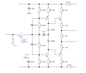
I am attaching the criticized original once again so that we know what you are philosophizing about!
Greetings Bernhard,
HBt.
Attachments
Last edited:
Please refrain from such stupid and discrediting comments.I would not have thought that you could formulate longer and coherent sentences, I like that.
👍
Otherwise I would have to contact a moderator.
Clear?
Let's go for a walk together in the moonlight and discuss the pros and cons, shall we?For further informations, ask Microcap
Perhaps you would like to suggest suitable small signal transistors under the new aspects, with regard to V_CE_0 and the lowest THD to be achieved. That would be nice and constructive of you.

I´m not "philosophizing"I am attaching the criticized original once again so that we know what you are philosophizing about!
However, your post #462 is very revealing...
Bye
Final post here:
Ask the pudding if that Vce is ok, otherwise add another volt by changing the bias network.
Ask the pudding if that Vce is ok, otherwise add another volt by changing the bias network.
It is solely your concern to poke fun /disturb in this thread, nothing more and nothing less - I find that very annoying.
Coherent and explanatory sentence structures are simply more helpful than chunks thrown in.
Thank you!
Bye,
HBt.
Coherent and explanatory sentence structures are simply more helpful than chunks thrown in.
Thank you!
Bye,
HBt.
That may be the case, but it should only serve as food for thought and not be used for insinuations. I think your intention is negative.However, your post #462 is very revealing...
Bye
If you would (really) stop bothering me now, that would be helpful and positive.
#
The post 462 expresses that you /we can and may accept other points of view. Nothing more and nothing less.

You're right; the Northmen don't like ... (and vice versa). But we shouldn't go into the inner-German issue here - it's a shame.
I prefer technical discussions
😉.
I prefer technical discussions
😉.
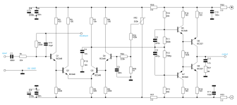
First of all, the original 1st stage was demonized - but it works, in the real setup it will not oscillate (because the author would have simply noticed that), even the selected transistors do not suffer a Vce breakdown (the author would also have noticed that).
But be that as it may, the forum did not demand a high-impedance emitter follower as a load for the LTP, but a voltage-amplifying emitter circuit -> I gave it what it asked for. And then it wasn't right either.
Of course, this has technical consequences - and so the similarity between the two circuits is only apparent. Initially, the common emitter resistor was criticized and the call for a current source / sink became loud - "Let her have what she wants, the Illsebill" ... "lass sie haben was sie will, die Illsebill" ! and so on, but there was one thing I didn't get involved with (changed) - and that was the output stage, because everything really revolves around this buffer.
#
Should I throw the project in the garbage can?
😢
🍿popcorn, I need popcorn!
Aha, but you belong to the triple B gang - now you suddenly want to enjoy the spectacle?
Curious - but ...
I'll go and get a cold beer
😉
Not at all - but I wasn't even talking about the so-called operating points or other voltage cases, which you were only too happy to imply with your question.How could static voltages be amplified?
Well, I've asked them several times and each time the result is the same: "There's nothing wrong with me", says the vanilla pudding. Old Spice, MC12, measurements and an understanding of the circuit confirm the dessert's statement.Ask the pudding if that Vce is ok, otherwise add another volt by changing the bias network.
But here we have repeatedly, but in a different form, hidden the fact that you can't understand the circuit or, more likely, can't accept that your world of suggestions doesn't knock my (HBt.) socks off.
You seem to have acceptance problems with the (for you too) low impedance dimensioning of the base voltage divider 33kOhm and 2k7Ohm, therefore you constantly and perpetually blather on about the (in your eyes) correct bias network of the original and even go so far as to claim that my (exactly as intended) dimensioning is harmful for the THD.
Well, in contrast to the original, my incarnation of the IP is not really intended to have a voltage-amplifying effect, but only the following emitter circuit - the choice of (high) quiescent currents is also exactly what I tended to do.
In the original, the high-impedance voltage divider of the collector circuit was also chosen by the author as it suited him - namely as the resulting ac load of (39kOhm/2) || r_in. In accordance with the TIM doctrine, he deliberately distributes the entire amplification over two shoulders.
I try to avoid this as much as possible. In the original you have to consider the complete second stage as a symbiosis ... in my case it's slightly different - and exactly as intended.
In the back of my head there is always a small signal equivalent circuit diagram; I hope this is also the case for you.
#
It's not worth arguing that I did something wrong, but you don't get tired (and post another stupid *.cir MC12 sketch), because: that's exactly how I wanted it! What was later to become of the handicrafts is another matter entirely. And, to be very clear once again, your contribution to the good of the project has been heading in the opposite direction right from the start. Zero gain, only loss, loss of nerves, time and joy ..!
So I'm totally fed up with your destructive comments ( also only MC12 fragments postings) - and that's very annoying.
In the course of the year I will have a fully functional stereo amplifier that follows the unconventional concept of this thread - the next heckling and diversionary maneuvers won't change that.
Has the /this message reached Bavaria's capital?
Bye, bye ... for today
HBt.
Last edited:
Is this to be understood as a daily postcard? Nice, but I can't say anything more about it - can't do anything with this /your objection at all.
😳
It would be more productive if you were to say openly what I'm doing wrong and also why, in contrast, you're doing everything right.
thx
Last edited:
- Home
- Amplifiers
- Solid State
- high performance 25W PowerAmp