Hi,
I am not suggesting you change your plans to building a Leach clone. Keep your project going as is.
All I was doing was stating what power is availaable from a 40+40Vac transformer using a triple stage EF with 3pair of MJL4281/4301. And this with all the voltage drops involved with running from a common supply rail throughout. It may give very slightly more if and when I regulate the front end.
PB2 said:
I suggest 10 ohm base stoppers for all the outputs. CFPs are a bit more fussy it seems. I do like CFP by the way.
MPSA42 is very low beta, 2N5550 is much better, they only see one rail or 70V worst case in your latest design.
C9 is shorted in your latest.
Hi Pete,
I have made some updates to the sub woofer amp schematic. Added base stoppers, changed to 2N5550 for the casode, fixed C9.
I also changed the output stage to CFP and reduced the devices from 4 pair to three (as these amps will not see a 4 ohm load).
I will do some of the testing you suggest on this version and get back with the results.
EDIT: Yeah, I missed the base stoppers on Q6 and Q15🙁
Attachments
Your CFP is not quite right, take a look at self or the elliot site.
You were looking for better devices, if your planing to buy specific devices, a dual for the diff amp will help, and with it cascoded, there's less than 10V Vce. You can always hand match them and thermally couple them, but it's never as good as a matched pair.
This paper discusses matching, and also indirectly why "bootstrapping" the cascode is important:
"Distortion in low-noise amplifiers" by Eric F. Taylor, Wireless World August, 1977 and also the September part 2 issue?
Might want to consider a dual J-FET.
It's coming along nicely otherwise.
Pete B.
PB2 said:Your CFP is not quite right, take a look at self or the elliot site.
Hi Pete,
I don't see what you're talking about...what did I do wrong? R6 and R37 too low? Too much current, I can increase these.
...a dual for the diff amp will help,
Do you mean a monolithic dual pair? Any suggestions? I have two such devices, salvaged from an old Pioneer amp. They are 2SC2291, with hFe: 250 (max 1200). I also have a couple of 2SA798 (PNP). These have a lot of miles on them, but to the best of my knowledge, they work fine. Worth playing with, or toss them out?
"Distortion in low-noise amplifiers" by Eric F. Taylor, Wireless World August, 1977 and also the September part 2 issue?
Do you have a copy to forward? I can't find it on the internet
Might want to consider a dual J-FET.
As little as I know about bjt's, I know less about fets. I'm willing to learn though.
It's coming along nicely otherwise.
Thanks 🙂
Hi John,
Check out figure 1a here:
http://www.dself.dsl.pipex.com/ampins/dipa/dipa.htm
I should probably mention that the EF output is looking fairly good with modern devices that have less beta droop than older ones. Either should be fine.
Yes a monolithic pair, the ones you have are probably fine, you say they have a lot of mileage. Some report that particularly diff pair devices become noisy over time, the only reason I can think of is static discharge when pluggin and unpluggin the input jacks. I see a lot of sparks during the dry winter weather. It's not a big deal, if you want to be fussy about it, it is the best way to go. I like the LM394 used in the 990, also the similar AD parts are fine.
Sure, I'll send it if you send me you email address.
Bipolars require while small, some base bias current which causes some offset at the input pins, they also have better noise performance with low source impedance. JFETs have virtually zero input current, and better noise performance with higher impedances. But their gain is lower so the distortion is usually higher. Just something to think about. There are plenty of examples, Bob Cordell's amp written up in the AES, it's at his web site, and many other examples here.
Pete B.
PB2 said:
The example I'm using is from Rod Elliot's P68 sub amp (the one that I built) here:
http://sound.westhost.com/project68.htm
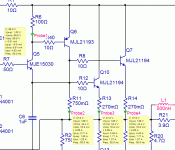
I have been playing with it though, as after you said it was flawed, I began to check some voltages and current. I found that the first output transistors (the ones in the loop with the drivers) were only delivering 350mA to the output (full power) while the other two were running 1.5A.
I found that by reducing the emitter resistors on the drivers, I could balance that load. I have attached a graphic to show what I'm talking about.
Is there any reason to keep the emitter resistors larger on the drivers? In this simulation, with these devices (MJL21193/94) this works very well. Better than a straight EF for these transistors.
Let me know if I got this all funked up.
BTW, it's jpheisz at rogers period com
Attachments
Hi John,
Yes now I remember seeing that at Rod Elliot's site, but that is like a 3 stage output stage where the first two are wired as CFP feeding an emitter follower. That's a big device to use as a driver, and I'm not sure what his justification was for it all. Perhaps he runs the CFP biased hot, as far as a driver goes, which helps with the crossover distortion issues.
The basic 2 stage CFP can usually be made to work well, especially with the newer high beta devices. I believe that a current limiting resistor would help protect the driver, either in the collector or emitter path. Ten to twenty ohms is probably about right.
I'd rather see the driver, work as another output device in parallel but if you can get it to work reasonably, then I suppose it's fine. I would not do it that way. Oscillation and crossover distortion are always potential issues with CFP so you might want to simulate and then decided which you prefer. You should also have a decent bandwidth scope ( > 100 MHz) to check for oscillation.
Pete B.
Hi,
the CFP driver is working in ClassA at low output currents.
If a big device is used then more bias current can flow in the driver and that extends the ClassA range of output currents.
Normally the optimum bias for a CFP is very low (maybe ~5mA) and this optimum bias is very close to the driver bias.
But, if the driver is set up to pass 200mA then I suspect that the optimum ClassAB bias is now raised to near the driver bias current.
Can anyone confirm whether any of this is true?
PB2 said:
Perhaps he runs the CFP biased hot, as far as a driver goes, which helps with the crossover distortion issues.
AndrewT said:
the CFP driver is working in ClassA at low output currents.
If a big device is used then more bias current can flow in the driver and that extends the ClassA range of output currents.
Hi Pete and Andrew,
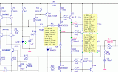
what I'm seeing is that this output stage seems to work very well with class B. This configuration is showing less than .009% THD at full output power. I have tried straight EF, and couldn't come close to that.
Below is a graphic with voltage/current probes in place to show what's happening at idle. With no signal Q5 is passing ~6ma and Q6 is passing 300mA. This is with my revised resistor values (attempt to share current load between these three output pairs).
The other two pairs of the output stage are delivering no current at idle.
I know that 306mA quiescent current is high, but is it a problem?
Attachments
MJL21193 said:
I have tried straight EF, and couldn't come close to that.
OK, scratch that. I've done better. Further work on the sim shows the EF out-performs this configuration.
I will re-do the schematic using a straight emitter follower output stage.
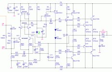
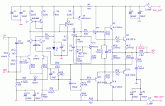
Getting back to the original plan, here is the updated schematic for the first amp.
I have decided to use the LM394 (supermatched pair) for the differential input (thanks Pete). These are rather pricey ($10.50 each), but save me the trouble of matching the BC550's and I can expect higher performance. These are a TO-5 package.
I have also replaced the output devices with MJL3281A/1302A. I will save the higher voltage MJL4281A/4302A for another project. Another possibility is the 2SC5200/2SA1943 pairs. I have a few of these kicking around.
How critical is it to match the output devices? The MJL21193/94 that I have came pre-matched (10 pairs), though I don't want to use those here.
I am getting to the board layout point on this, so if there are any obvious defects or other suggestions, now would be the time to let me know.
Please look it over and help a rookie out.🙂
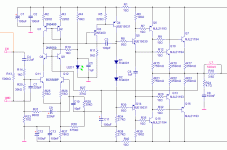
Attachments
Hi,
I would swap the order of R32 & C12 and bypass across C12.
Allow for an emitter resistor on Q4.
Allow for a LED//cap from Q6&7 base to junction of R26 & R27.
Allow for a series cap + R from +ve rail to Q1 collector.
Allow R+C in parallel to R29//C13.
All of these are optional but open up the possibilities to correct any misbehaviour.
Is there any possibility that LED1 needs to be doubled up for more voltage on the cascode? Maybe allow a second LED location?
My usual advice, make all caps locations with multiple pin pitch.
AndrewT said:
Is there any possibility that LED1 needs to be doubled up for more voltage on the cascode? Maybe allow a second LED location?
Hi Andrew,
In the sim, I'm seeing a steady 1.6Vdc at the base of Q6 and Q7. Is this right?
Before I do a board layout, I will prototype this on the breadboard. Here I should be able to weed out any bad behavior.
Are there any other areas of concern? How about the polarity of C14? In the sim, it works equally well either way.
Your opinion on the output transistors - make a difference if I use the Toshiba devices? Also, is matching the output pairs critical for best performance?
Hi, steady voltage on Q6&7 bases does not sound right.MJL21193 said:In the sim, I'm seeing a steady 1.6Vdc at the base of Q6 and Q7. Is this right?.............Are there any other areas of concern? How about the polarity of C14?
If LED voltage alone then, yes, steady.
But, I thought the purpose of R28/R6 was to swing the cascode voltage in the same direction as the NFB signal coming back to the inverting input at U1 base. I thought the cascode would track the input voltage but of opposite phase, otherwise all these extra components are doing nothing.
Similarly R36 should be modulating the bottom (tail) of the LTP.
Like I said a while ago I don't understand this aspect of the circuit but I can see what should be happening, I just can't see the consequence.
C14 orientation.
imagine the amp in quiescent mode.
What voltage is on the output rail?
What voltage is on the -ve supply rail?
What voltage is at the junction of R33 & R38?
What voltage is across C14?
What polarity?
Now move the voltage quickly on the output and return it quickly before C14 charges/discharges significantly. What happened to the voltage at the +ve end of C14?
What happened at the -ve end of C14?
You should be able to plot this in the sim.
You should see this effect change as you lower the signal frequency.
Remember you should be checking the reports of the sim manually to ensure that it is not misleading you.
AndrewT said:Hi, steady voltage on Q6&7 bases does not sound right.
If LED voltage alone then, yes, steady.
But, I thought the purpose of R28/R6 was to swing the cascode voltage in the same direction as the NFB signal coming back to the inverting input at U1 base. I thought the cascode would track the input voltage but of opposite phase, otherwise all these extra components are doing nothing.
Sorry, that's dc voltage, ac voltage fluctuates depending on power output. From 500mVpp @ 4watts to 3.1Vpp at full output.
My lazyness is showing through with C14, I was trying to get someone to do my thinking for me.
I'm not giving you the answer. Think of it as your homework. 😉MJL21193 said:My lazyness is showing through with C14, I was trying to get someone to do my thinking for me.
AndrewT said:I'm not giving you the answer. Think of it as your homework. 😉
No, I've put my brain in gear and have come up with the answer. It's oriented correctly in the schematic shown. Somehow, it got inverted during all of the tinkering and I was confused.
I'm looking to start prototyping this coming week. In your eyes Andrew, does it look good?


- Status
- Not open for further replies.
- Home
- Amplifiers
- Solid State
- Help with this amp? A patchwork product of simulation