as you may expect - it depends. first question is if you understand the technology differences between the MOSFETs? You can see from the datasheets that they are NOT drop-in replacements at all.
BTW, your question reminded me of a very gentlemanly discussion quite some years ago between Nelson Pass and Charles Hansen (RIP) that touched on some differences between VMOS and Lateral MOSFETs. It would be useful reading for such a venture. If I find a link, I'll share it. I suspect someone else will beat me to it. And, although we've lost A LOT of the incredible expertise that visited this site over years past, there is still a lot of really good stuff around that if sorted through and studied can be helpful for budding designers as well as experts - it can save one lots time, save some PCB revs and avoid some burned up parts ! 😉

Hi, thanks for you repli. I will try to answer your questions, honestly and clearly:for the OP: might be worth it to take a step back for a moment and clearly confirm your objective(s):
What your immediate goal? Quickly build a working amp to use in your system? Or ...
start to develop design skills to design your own amp at some point in time?
What is an honest assessment of your current skill levels? If you search around here a bit, you will see that designing, building and testing a high performance MOSFET amp that is not an already "tried and tested" design or even a kit is not trivial. The Profusion Lateral MOSFETs are similar but NOT identical to the old Hitachi/Renesas Lateral power MOSFETs and, as you've found out already, they're not drop-in replacements all Lateral MOSFET designs without taking into account the subtle differences if the original designer has not already done that for you. Not trying to discourage; just want to help mitigate frustration and increase chances of success by helping you select realistic goals and better aim at them ....
My first goal is to build an amplifier that works like my system. It's not the first one but in the other occasions were easy projects that it hasn't given me many problems.
At the same time I want to acquire skills, not to design, but to know how to solve problems in future assemblies.
My level of knowledge, electronics technician, mainly in repairing communications equipment. I have always been enthusiastic about the world of audio, amplifiers and loudspeakers, in fact I have built loudspeakers too.
It is true that designing, assembling and testing is not easy, but as a technician I like to try. In this case I bought the Exicon because Profusion told me that they are the replacements for Hitachi, and it has become clear to me that this is not the case. After a lot of reading and looking around the forum, I have seen some great projects with these MOSFETs, assuming that they are not all the same. That is why I am asking the question and trying to save the investment in components.
I thank you for your honesty, and I also reply that my goal is to enjoy a self-made amplifier.Not trying to discourage; just want to help mitigate frustration and increase chances of success by helping you select realistic goals and better aim at them ....
Thank so much.
47 ohms both on positive and negativ rail.
I just checked the amp in TINA with somewhat other transistors and it worked well but only without C5.
I changed R13 and R15 to 47 ohms and R16 to 33 ohm.
It doesnt have so much open loop gain so the distortion value will not be so good but it sounds better than expected due to mosfets instead of bipolar output transistors. I used 2 of them a few years as PA amplifier for a rock band.
I think mine were about 0,05% distortion at full power.
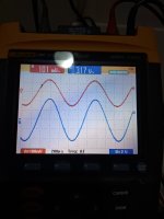
Hello friends, I continue with the tests of the different configurations. 😀.
At the moment, this is the best option I see for this project. What do you think of these measures?
Image1: how Flikoman describes without C8
Image 2: how Flikoman describes without C8, and C6-C7 to 150pF.
I continue with some more tests,
This option doesn´t work.You may try these mods
This option doesn´t workThat's roughly what I've got.... cheers Frank
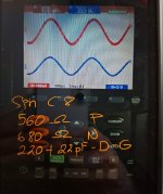
This option work, I think well, I add oscilloscope image.Use 560R (P) and 680R (N) gate stoppers and a zobel across D-G of the Exicons (220R + 22pF).
At the moment, this is the best option I see for this project. What do you think of these measures?
Image1: how Flikoman describes without C8
Image 2: how Flikoman describes without C8, and C6-C7 to 150pF.
I continue with some more tests,
Attachments

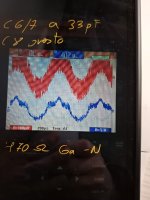
This option the test is not clear, because the measurement is with C8 on, now I don't remember if I test it without C8.I did a quick and dirty simulation in ltspice, the gain and phase margins are quiet low, given the board layout it maybe partially unstable given the right conditions. Also with no output inductor, just connecting a loudspeaker would most likely cause the amplifier to go into oscillation.
The main contributor to this is the phase lead capacitor (C8) across the feedback resistor R11.
Unity loop gain is approximately 5MHz, gain is only -10db @ approximately 9MHz at 180 degrees phase.
The simulated gain/phase margin is approx 9db and 40degrees, probably worse with the real circuit board layout.
Removing C8 improves the gain and phase margin to approx 20db / 62 degrees, the loop gain at 20KHz (33db) is unaffected.
The simulated unity loop gain is now 760KHz.
Other changes:
R21/R22 - 470R
Leave R23/R24 at 270R
Leave C6/C7 at 33pf
As suggested move the gate resistors as close as possible to the mosfet gate pins. I would also add a output inductor to the amplifier approx 1uH -2uH.
I do it egain.
This is the measurement, oscillation also affects the input waveform.
Attachments
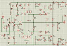
Hello again, after testing and a lot of reading, I have found a stable configuration for this design. This is the attached schematic. The option mentioned by Flikoman with the Zobel network between D-G, is the best option, but after reading the design recommendations with the Exicom Mosfet, they recommend gate resistors between 150-470 Ohm, the normal is 220 P channel and 330 N channel.
I have mounted the latter because according to the ‘Aplication Notes’ above 470 can affect the slew rate. With 220 and 330 Ohm in the gate resistors of the Exicon Mosfet, as measured by the oscilloscope, correct. But in audio tests it produces a sputtering in the mid-high frequency range. I changed them to 330 on P and 440 on N, everything sounds ok.
Looking again at the average Bias in the Source resistors, for the same channel (P, N), there is a variation from one resistor to another in the order of 0.6-0.7 volts. I put all the gate resistors of the same value, 330 Ohm, the Bias voltage remains similar from one resistor to another, only 0.1-0.2 volts variation.
What do you think about this? What resistors would you mount?
Translated with DeepL.com (free version)
Attachments
Connect it to a speaker and feed a sine wave. Sweep the frequency across the frequency range and see if you can reproduce the “sputtering”. Once we know when it happens and what it looks like, it’ll be easier to figure out what’s going on.
I would also simulate it to see if you have any resonances in the CLG and OLG gain plots.
I would also simulate it to see if you have any resonances in the CLG and OLG gain plots.
220 ohm stopper resistors should fix oscillation issues with the Excicon MOSFETs. I don't particularly like the Hitachi schematic from the app note, as I don't believe there's enough current in the second differential stage to effectively charge the output MOSFET gates. Here's the thread for the modified Hitachi amp circuit:
I have had some peeves with the classic Hitachi Lateral mosfet amplifer designs from the app notes in the early 80's, mainly due to the limited amount of current available from the 2nd differential stage for charging the gates of the output lateral mosfets. I sorta had my way with the original design and came up with one utilizing a Pmos input, bipolar second differential stage, and a follower stage to drive the output lateral fets. Since I don't have lateral fets in my PSpice bag of tricks, I used a Vgs multiplier for bias and a complementary vertical fet output stage. In practice, I...
- wrenchone
- Replies: 33
- Forum: Solid State
Last edited:
I have also had problems with high frequency oscillations at tens of MHz using Exicon MOSFETs
I prototyped a Class I circuit using a pair of original Hitachi MOSFETs, 2SK133 and 2SJ48, bought many years ago and it worked OK with sensible gate resistors. When I designed a PCB using the Exicon (ECX10N20 and ECX10P20) I had high frequency oscillation, typically around 50 MHz. I tried various gate resistors, power supply decoupling and Zobel network values but under certain conditions of load or no load oscillation occurred. I found it hard to track down because it came and went seemingly at random times and various loads.
In desperation I tried a ferrite bead in series with the drain (Murata BLM31SN500SH1), a Zobel network of 1 ohm in series with 10 nF for a low RF impedance to common, plenty of hf power decoupling and no gate resistor and it worked!
My guess is that the bond wire and chip layout inductance along with the inherent capacitances make the parts prone to the high frequency oscillation. I am open to any ideas that have been proven to work in practice.
My schematic is in this thread:- 'Amplifier based on the Kendall Castor-Perry's Class I output stage'.
High-frequency response of lat-FETs is scanty specified and widely unknown imho.
So I do not expect spice models telling the truth here.
Phase shifts between gate input and source outputs rise at frequencies in the MHz region.
Stabilizing Boucherot snubbers, various gate resistors etc thus are pure trial and error.
This is what I experienced when designing Lat-FET class AB-amps.
To make a long story short -
You avoid a plethora of stabiliy problems if you close the feedback loop for high frequencies
NOT at the common source output, but at the VAS output / gate driver output.
In that case, C8 must be re-routed accordingly while R11 stays untouched.
By using this simple trick my latFET amp ist stable without any snubber at all.
This should work, but they must be very close to the gates. Several cm of track or wire to the stopper is enough to turn the lateral into a radio transmitterthe normal is 220 P channel and 330 N channel.
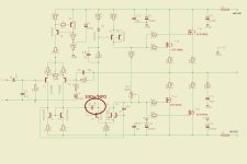
The source connection of the MOSFET needs protection from capacitive loads. The small inductance of a wire-wound resistor as shown can provide this, a 0R22 value will do more than 0R1 in that regard. The gate stopper resistors will do better if there is a low pass filter capacitor between the gate and the source. The gate stopper resistors could be increased in value up to 330R and the capacitor value introduced between gate and source, decided by trial and error. This circuit looks tidier for stability as there is only one capacitor around Q4 however the value might need to be changed. This could be connected from the collector of Q4 to the base of Q2 as has been indicated in another input suggestion. I would not recommend a lead capacitor in parallel with the feedback resistor as any hf instability due to the load will be introduced to the systemThis one looks like yours, is simpler and works no prob with Hitachis and Exicons. If you pair Q1 and Q2 well, offset will be low.
View attachment 1406302
Last edited:
Great. I try it.Connect it to a speaker and feed a sine wave. Sweep the frequency across the frequency range and see if you can reproduce the “sputtering”. Once we know when it happens and what it looks like, it’ll be easier to figure out what’s going on.
I would also simulate it to see if you have any resonances in the CLG and OLG gain plots.
ok,I'm going to change D3, C4 is now nichicon, but I'll try to change it.D3 is backwards, C4 should be Nichicon UES bipolar type - 220 to 470 uf / 25/35 volts - bigger uf is better and higher voltage is better
Thank you, but I don't understand very well, if you show it to me in a drawing. I could try it.High-frequency response of lat-FETs is scanty specified and widely unknown imho.
So I do not expect spice models telling the truth here.
Phase shifts between gate input and source outputs rise at frequencies in the MHz region.
Stabilizing Boucherot snubbers, various gate resistors etc thus are pure trial and error.
This is what I experienced when designing Lat-FET class AB-amps.
To make a long story short -
You avoid a plethora of stabiliy problems if you close the feedback loop for high frequencies
NOT at the common source output, but at the VAS output / gate driver output.
In that case, C8 must be re-routed accordingly while R11 stays untouched.
By using this simple trick my latFET amp ist stable without any snubber at all.
- Home
- Amplifiers
- Solid State
- Help with an oscillating amplifier with Exicon mosFET ECF10P20 & ECF10N20