
Hi there, I am compiling the components for the changes you have told me about. Because I would like to test them all, and of this way learn more about amplifiers. But in case of the @fschmdt65 there are two schemes, could you tell me what the diferent is?, which one do I use?
Thank so much
Thank so much
@carcotado ,hi,soryy to answer late,i've got problems with mu pv inverter....
The second scheme is what i've got and this is really working well.I have seen you use the metal round exicon.Be careful with cables to the board,this might lead to oscillating .I would go with your outlay first,checking evetything what could trigger oscillating.Try a view things out and carefully advance.Sometimes it's only a matter of trying .GOOD LUCK for now,Frank
The second scheme is what i've got and this is really working well.I have seen you use the metal round exicon.Be careful with cables to the board,this might lead to oscillating .I would go with your outlay first,checking evetything what could trigger oscillating.Try a view things out and carefully advance.Sometimes it's only a matter of trying .GOOD LUCK for now,Frank
Yes, probably now that I read the schematic properly. Never mind…T10 and T11 have a Miller cap, but T8 and T9 don’t. Is that by design?
Thank so much.
I understand @fschmdt65.
@davidsrsb that´s true, I´ll show this.
@njswede, I know the schematic as follows.
I understand @fschmdt65.
@davidsrsb that´s true, I´ll show this.
@njswede, I know the schematic as follows.
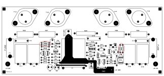
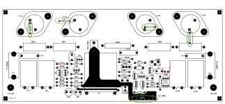
Here is layout.You haven't told us anything about your circuit layout. In particular those gate stopper resistors need to be very close to the mosfet gates or the outputs will oscillate all by themselves
Whith red circled in red, are gate resistors.
Attachments
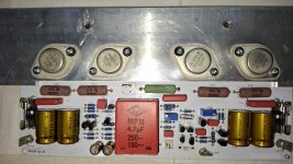
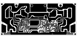
They are bit far away and the supply decoupling is poor too.
A single via connecting GND on the two layers is weak.
A single via connecting GND on the two layers is weak.
@davidsrsb, I think, do you mean something like this. resistance close to gates, and more pads betwen two layers of GND.
but I don´t understand "supply decoupling is poor"
Could you show me it, please.
but I don´t understand "supply decoupling is poor"
Could you show me it, please.
Attachments
I did a quick and dirty simulation in ltspice, the gain and phase margins are quiet low, given the board layout it maybe partially unstable given the right conditions. Also with no output inductor, just connecting a loudspeaker would most likely cause the amplifier to go into oscillation.
The main contributor to this is the phase lead capacitor (C8) across the feedback resistor R11.
Unity loop gain is approximately 5MHz, gain is only -10db @ approximately 9MHz at 180 degrees phase.
The simulated gain/phase margin is approx 9db and 40degrees, probably worse with the real circuit board layout.
Removing C8 improves the gain and phase margin to approx 20db / 62 degrees, the loop gain at 20KHz (33db) is unaffected.
The simulated unity loop gain is now 760KHz.
Other changes:
R21/R22 - 470R
Leave R23/R24 at 270R
Leave C6/C7 at 33pf
As suggested move the gate resistors as close as possible to the mosfet gate pins. I would also add a output inductor to the amplifier approx 1uH -2uH.
Why is T4 and T3 wired as a current mirror? With a emitter coupled pair (T7 and T10,11) T4 should not be wired as a diode...
Most amplifiers I've seen use an emitter follower to drive the Mosfets, and have a zener and diode stopper to protect the gates of the outputs. (Hafler 220 type output stage)
Most amplifiers I've seen use an emitter follower to drive the Mosfets, and have a zener and diode stopper to protect the gates of the outputs. (Hafler 220 type output stage)
That's why i suggested re-routing C8The main contributor to this is the phase lead capacitor (C8) across the feedback resistor R11.
There are a few things worth to discuss in the schematic.
1. The T3 and T4 does not add to the function of the circuit. The input admittance of T7 and T10 + T11 is a little over 400 ohms. ( 21mv x HFE / Ic) So the 2,7k of the R7 and R9 dont take that much of the signal. Just take away T3 and T4 and add a jumper E - C. Change R16 to make 20 mA through it.
2. The T8+9 and T10+ T11 might have very different currents. Normally the base voltage of the same type transistors can differ 60mv ( sometimes even more).
That means 10 times higher current in one of them. Here you have pretty strong transistors so it would be better to only use one. To manage the heat you need a cooler. There are clip on coolers but you can also use an inch of venetian blind lamell. If you cant find that you can use the smallest coin you can find. Just glue it with epoxi (fairly good heat conductor) to the flat side of the transistor. R13 and R15 should have the same value = 2x R16.
3. The C5 and C6 can lead over high frequency signal from the positive power supply rail to the base of T7 and via emitter and T10+11 to cause self oscillation.
To get rid of this take away C5 and disconnect the C13 and C9 from positive power supply rail for high frequencys. 47 ohms between C9 and C11 will do the job. It is the same problem between C10 and C 12 so 47 ohms there will also be good. There is a possibility you can use the C5 if you move over C6 to T8+9 B-C
4. I would add a 10v zenerdiode G-S on T13 and on T14 for gate to source voltage protection.
From the other suggested improvements I would only keep The 100nF between T8+9 C and T10+11 C.
I am not sure if the values of C6 + C7 or C8 are ideal. When I build this in 1974 I used 47 pF for the Miller integrators and 47k with 4,7 pF for feedback.
Without the 47ohms in the supply rails you will not get a proper simulation in Spice. And even worse with C5 as in the original schematic. It is the high frequency impedance in the leads that mess it up.
R21 to R24 will probably work better with 100 ohms.
Last edited:
Thank you very much for your answer, I will buy the components to test the different options.
I have no knowledge of design, and I have some questions about your recommendations.
Thank you again for the answers, but I have no knowledge of design and therefore I have other doubts that I would like to know and learn.
I have no knowledge of design, and I have some questions about your recommendations.
I understand that the design and placement of the components is not well...? What do I need to change?given the board layout it maybe partially unstable given the right conditions
I don´t know the answer.Why is T4 and T3 wired as a current mirror?
Sorry 🙏 but, I don´t understand.You appear to only have those electrolytics in the supply rails and they are far from the output devices. You have to think about where those high Class B currents are flowing and also about self resonant frequency of the decoupling
I desconnect C13 and C19, and do not connect it anywhere? and R 47Ohm, only positive rail?To get rid of this take away C5 and disconnect the C13 and C9 from positive power supply rail for high frequencys
Thank you again for the answers, but I have no knowledge of design and therefore I have other doubts that I would like to know and learn.
Put gate stopper resistors on the solder side of the pcb.
Cut resistor leads down to 5mm on one side and solder directly to the gate leads, cut the gate traces under the resistor bodies and solder the other ends on the pcb traces. Install jumper wires in former resistor positions.
Cut resistor leads down to 5mm on one side and solder directly to the gate leads, cut the gate traces under the resistor bodies and solder the other ends on the pcb traces. Install jumper wires in former resistor positions.
for the OP: might be worth it to take a step back for a moment and clearly confirm your objective(s):
What your immediate goal? Quickly build a working amp to use in your system? Or ...
start to develop design skills to design your own amp at some point in time?
What is an honest assessment of your current skill levels? If you search around here a bit, you will see that designing, building and testing a high performance MOSFET amp that is not an already "tried and tested" design or even a kit is not trivial. The Profusion Lateral MOSFETs are similar but NOT identical to the old Hitachi/Renesas Lateral power MOSFETs and, as you've found out already, they're not drop-in replacements all Lateral MOSFET designs without taking into account the subtle differences if the original designer has not already done that for you. Not trying to discourage; just want to help mitigate frustration and increase chances of success by helping you select realistic goals and better aim at them ....
So, @mlloyd1 if I may hijack the thread for just a minute. I recently designed and built a MOSFET amp based on IRFP(9)240 and it came out great. Loads of phase margin and it sounds lovely. I've been tossing around the idea of building an Exicon-version of it (if they ever come back in stock). An I in for an uphill battle if I want to do more or less a drop-in replacement? It's a fairly simple design with some similarities to Blameless.
- Home
- Amplifiers
- Solid State
- Help with an oscillating amplifier with Exicon mosFET ECF10P20 & ECF10N20