Can you measure the DC voltages coming out of U13 with the present circuit? If it fits in the OPA1632 input common mode range and if the offset is small, maybe you don't need any capacitors.
I think about 12 uF per side should suffice for 5 Hz, by the way.
I think about 12 uF per side should suffice for 5 Hz, by the way.
Hi Marcel,Can you measure the DC voltages coming out of U13 with the present circuit? If it fits in the OPA1632 input common mode range and if the offset is small, maybe you don't need any capacitors.
I think about 12 uF per side should suffice for 5 Hz, by the way.
I will do the measurement anyway, despite the fact that according to the datasheet the Input common mode range would be -10.5...+11V (at my +/-12V supply which is also supplied to the I-V stage feeding the buffer...). Another point came to mind: There is no coupling cap in the existing circuit. I'll also do some more layout analysis to verify this.
I'll be back.
Winfried
It doesnt need one does it? it sums the balanced output before the PGA doesnt it? this would remove the common mode DC of course
Well, I've further analysed the actual DEQX circuitry today. It clearly employs DC coupling into the stages after I>V. I'll measure the DCV at the I>V OpAmp output anyway, so I know facts instead of speculating 😉. So, if DCV is not "outrageous" as we expect, the Vocm function of the OPA1632 will handily reference the differential outputs to GND 👍😀
BTW1: I also confirmed that the circuitry around and after the 2310 Volume control is really not needed for my application as all the follow on stuff is buffering for add on boards or cinch outputs 😀
BTW2: The cinch outputs have an electromechanical muting function, so I will use their control signal to feed the "Enable" function of the OPA1632 for this purpose 😀
Greetings,
Winfried
In my experience the opa1632 doesnt servo its output to ground just because you tie the VOCM cap to ground, well it does, but that doesnt necessarily remove DC offset. it references the output to it, but that just makes the output GND -> AC plus common mode DC present. instead of level shifting the whole output as it would if you referenced VOCM to say +2.5VDC , which would shift the whole output, including the DC, making it +2.5VDC -> + AC + common mode offset. ie. its not a servo; if you want a servo, add a servo.
Maybe i'm misunderstanding what you are saying though.
Maybe i'm misunderstanding what you are saying though.
you can think of it as a 3rd input, non-inverting that is used solely for shifting the common mode voltage output. It allows you to match/level shift the common mode offset to match a following stage; usually an ADC, so that the AC output swings around the same offset as the ADC input and as a result stays within the most linear range of the ADC input common mode voltage (not sure if they call it a compliance voltage in ADCs). That wont cancel DC; as it will still ride on top of whatever that new 'GND' voltage reference is. You can make an attempt to level shift down by the same amount as the input DC + gain is offset 'up' by applying a negative voltage to VOCM, or by using asymmetric supplies, but as the DC normally fluctuates some, its not a very good solution IMO, as it wont be constantly adjusting, as a DC servo would.
Hi Inspector,
and thanks for your thinking! It's a bit hard for me to map your input to my application, so let me explain it to you:
The OPA1632 is supposed to drive a balanced (or symmetrical) Signal Line from the DAC to the balanced Input of a Power Amp, where a studio grade differential signal input is being driven. The CMRR of that input is specified >100dB which I think may help, although I don't know the common mode input voltage range... But knowing that the Input Amp is supplied with +/-15V even that (I think) should be no issue.
Also, the OPA1632 datasheet states under 8.1 that a low impedance voltage at Vocm sets the DC Output voltage. So, my assumption is so far, that if I connect to GND, then the output DC is very close to Gnd. Leaving Vocm open, would set DC Out to mid-Supply which is not what I want, despite knowing that my +/-12V Supplies are accurate to a few mV or so.
Anyway, your thoughts, considering my feedback, would be valuable. I'm here to learn and to do this with as few understood compromises as possible 😉
Regards,
Winfried
An output common mode loop forces the average of the two output voltages to some value, so with VOCM = 0 V, the output voltages are (ideally) each other's opposite, as you would like them to be.
This doesn't suppress differential offset. Having one output at Vdoff/2 and the other at -Vdoff/2 perfectly satisfies the criterion of the common mode loop. I would therefore be interested to know both the common mode voltage and the differential offset coming out of the transimpedance stage.
This doesn't suppress differential offset. Having one output at Vdoff/2 and the other at -Vdoff/2 perfectly satisfies the criterion of the common mode loop. I would therefore be interested to know both the common mode voltage and the differential offset coming out of the transimpedance stage.
OK friends,
all you state is really interesting and instructive! But just a gentle reminder that the OPA1632 circuit part is in design and not yet built. I'm also unfamiliar with circuit simulation, so I may have to try this out physically.
With all your valid concerns in mind: I have based the design on the application proposals of the component vendors and think these should work. Well, I conceed that tweking may become necessary after measuring the behavior as you suggested.
For what its worth, I have created a 70x45mm stereo buffer board. Actually, one version assumes the OPA1632 soldered on a DIP8-adaptor, so it would be more easily servicable if need comes up... So, here's my first hit at a 2-sided Sprint layout for your valued input.
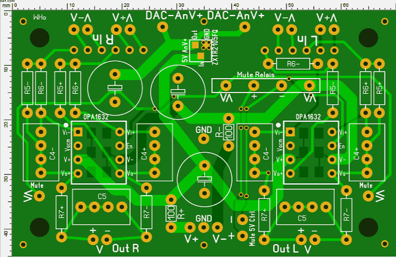
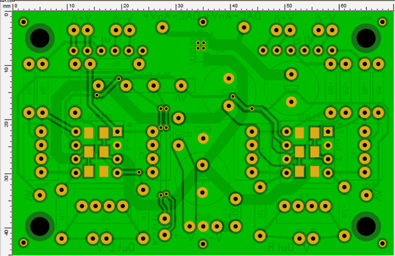
An optional Reedrelay is on-board for the muting funktion with the chip's Enable function, also I have placed an optional 5V Regulator (feeding from the +12V rail) to potentially feed the AD1853 analog with 5V it needs (and not use the system's internal 5V for this).
Please let me know your proposals, objections or concerns, if any.
Hi Marcel,
not being 100% certain about the correct nomenclature: Is the "transimpedance stage" the I>V stage or the buffer I'm designing?
Regards,
Winfried
all you state is really interesting and instructive! But just a gentle reminder that the OPA1632 circuit part is in design and not yet built. I'm also unfamiliar with circuit simulation, so I may have to try this out physically.
With all your valid concerns in mind: I have based the design on the application proposals of the component vendors and think these should work. Well, I conceed that tweking may become necessary after measuring the behavior as you suggested.
For what its worth, I have created a 70x45mm stereo buffer board. Actually, one version assumes the OPA1632 soldered on a DIP8-adaptor, so it would be more easily servicable if need comes up... So, here's my first hit at a 2-sided Sprint layout for your valued input.
An optional Reedrelay is on-board for the muting funktion with the chip's Enable function, also I have placed an optional 5V Regulator (feeding from the +12V rail) to potentially feed the AD1853 analog with 5V it needs (and not use the system's internal 5V for this).
Please let me know your proposals, objections or concerns, if any.
Hi Marcel,
not being 100% certain about the correct nomenclature: Is the "transimpedance stage" the I>V stage or the buffer I'm designing?
Regards,
Winfried
I'm going to have another go at explaining what I was talking about, as I myself screwed up the nomenclature in one part. the description was fine, but my use of common mode to refer to the input DC was incorrect.
Yes, it will swing symmetrically around whatever voltage is set at the OCM pin, whether that is GND, or some small deviation from that (you are limited by the linear range), provided the rails will accomodate that, but what i'm saying is, that signal will still ride on top of the differential mode DC voltage offset from the DAC, per pin.
I know you havent built it yet mate; this is info you should take into account and doesnt only apply to opa1632, at least the concepts do. i'm also adding it here in this thread for anyone else that may end up here and IS using opa1632, LME49724 or similar FDA for IV. In fact the issues will be there for using it as a buffer too, as you will follow a stage that has DC and you may wish to DC couple (or not)
Summed, ideally it will all cancel still, but before-so, the DC is there nonetheless. Maybe I need to illustrate what I mean? VOCM does not cancel/servo out the DC, it servos the mid point, but all that does is shift the differential DC present in the signal, not remove it. Summing will remove it.
My description of it as common mode DC is not correct; it was late, but I thought I described the phenomenon itself fairly well? hell I dunno, i'm not a doctor 🙂 sometimes the lingo in my late night stream of consciousness gets away from me; my apologies. All other uses of 'common mode' in my post were correct, but not here. I guess its more correctly called dual differential mode DC, as common mode, as Marcel says, speaks of the relationship/average between them ie, it speaks to the whole, rather than the elements.
Just for example, with ES9018 (CMOS based dac, +3.3V AVCC reference) , followed by an opa1632 with the VOCM tied to ground, Each output to ground will contain the AC signal, riding on ~ +1.65V multiplied by any transimpedance gain/voltage gain. Measured across the +/- outputs it cancels to ~0VDC. I'll have to dig out one of my opa1632 boards and measure exactly and see what deviation from AVCC/2 is present. Thats all well and good for most circuits, but certain DC coupled power amp designs may end up with 40 or 50V of differential DC per pin at the output. Perhaps i'm more concerned with that than I need to be? It will depend on the topology, whether you can even consider playing fast and loose with it.
I dunno, the designs i'm working on for IV with opa1632 and THS45XX fully differential amplifiers in a few board layouts are all complicated by this DC, as for best performance with ESS. The idea is to force the output of the dac and the input to the IV node to share the same ideal voltage, where it best fits within the DAC AND the opamp linear compliance voltage region. in some low gain circuits may as well not be there, as it sums at the speaker/headphones or perhaps a differential input of an amp, but it makes me uncomfortable in amps with significant voltage gain; it will also fairly quickly eat up the output linearity and at worst clip and cause all sorts of ugly. the various methods of removing it, after very deliberately forcing it to be there, particularly DC coupled ways, have been something of a special interest of mine. I very much enjoy the 'symmetric' nature of these FDA's, electrically and WRT to physical layout. they allow very clean and also clean looking designs.
I would avoid using opa1632 on a dip adapter. its really not appropriate IMO. it isnt a super fast opamp, but it isnt super slow either at 150MHz bandwidth IIRC. are you using bipolar supplies? you should add a 0805 size ceramic decoupling cap of 0.1uf -> 1.0uf across VOCM->GND; this will improves noise performance vs just tying it to ground and it also provides a handy spot to add bias if required that you wont have if you just tie it to ground, without lifting a pin or cutting a trace. if you want the opa1632 to swing around 0V VOCM, setup like this, it will act to set VEE- -> VCC+ /2, which with symmetrical supplies will settle to 'GND'. With single supply it will sit VCC+/2 but not sure how I would decouple that, I would probably force a voltage of that in single supply mode and decouple/bypass that to ground, rather than leaving it floating (I have not done a lot with single supply with opa1632; as the performance is a bit lower)
The film caps for decoupling the rails, at the bottom of an adapter are going to be pretty much useless IMO. You may think you are following the application schematic, but the layout recommendations are not satisfied. i'll have a bit more of a look after lunch and provide a bit more feedback.
I hope I did better this time.
Last edited:
Regarding the coupling caps, there can be a tradeoff between SQ and elegance in some situations. If you want a small, high quality DC removal cap, then you need a high input impedance load following the cap. Otherwise the cap would have to be impractically large. A Fet buffer stage after the cap might allow you to use a very good polypropylene or polystyrene and foil cap. However, a nice Fet buffer might work best with a higher rails voltages than you have now. Also, you might need to servo it if you want lowest DC offset at the output. Sorry.
The above having been said, the easy answer to your problem might be to try a Panasonic FM electrolytic with a .01uf Wima FPK2 (or similar) in parallel. Not going to sound like polystyrene and foil, but it can sound surprisingly good. If you don't like the sound of FM you might try FC. Given the other imperfections of the circuitry I would probably go with the simple solution.
The above having been said, the easy answer to your problem might be to try a Panasonic FM electrolytic with a .01uf Wima FPK2 (or similar) in parallel. Not going to sound like polystyrene and foil, but it can sound surprisingly good. If you don't like the sound of FM you might try FC. Given the other imperfections of the circuitry I would probably go with the simple solution.
Hello Inspector,
no criticism from my side at all! On the contrary, I do learn a lot from your extensive descriptions!
Well, the first layout I made was with the SMD OPA on the board without adaptor and as you recommend this over the adapter solution, I'll share it here:
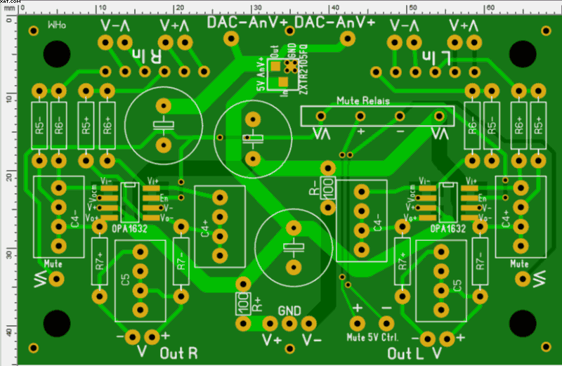
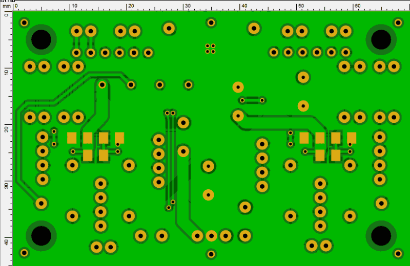
As on the adapter, I have placed the 100n NP0 decoupling Caps on the back side under the IC connected with vias and hope this is acceptable. Also, as the back side is supposedly a Gnd plane, I have tried to place most component connections on the upper side. There are some vias in the supply and signal lines to keep Gnd paths short and low impedance. Not sure this is the right approach, but it made sense to me anyway.
Next on my part is measuring the DC voltages you requested. Here's where I think you recommeded to measure:

DC Values to document as far as I understand:
A>Gnd, B>Gnd, A>B, C>Gnd, D>Gnd, C>D, E>Gnd, F>Gnd, E>F
These values for the R and the L circuitry.
Briefly confirm and I'll go with that.
Hello Mark,
thanks for your input! So far I'm using Panasonic low ESR organic polymer Electrolytics in Supply buffering together with 100n NP0 ceramics. As this thread has developed, it seems I may be able to avoid coupling caps, but if they're needed, I'll consider your recommendations.
Regards,
Winfried
no criticism from my side at all! On the contrary, I do learn a lot from your extensive descriptions!
Well, the first layout I made was with the SMD OPA on the board without adaptor and as you recommend this over the adapter solution, I'll share it here:
As on the adapter, I have placed the 100n NP0 decoupling Caps on the back side under the IC connected with vias and hope this is acceptable. Also, as the back side is supposedly a Gnd plane, I have tried to place most component connections on the upper side. There are some vias in the supply and signal lines to keep Gnd paths short and low impedance. Not sure this is the right approach, but it made sense to me anyway.
Next on my part is measuring the DC voltages you requested. Here's where I think you recommeded to measure:
DC Values to document as far as I understand:
A>Gnd, B>Gnd, A>B, C>Gnd, D>Gnd, C>D, E>Gnd, F>Gnd, E>F
These values for the R and the L circuitry.
Briefly confirm and I'll go with that.
Hello Mark,
thanks for your input! So far I'm using Panasonic low ESR organic polymer Electrolytics in Supply buffering together with 100n NP0 ceramics. As this thread has developed, it seems I may be able to avoid coupling caps, but if they're needed, I'll consider your recommendations.
Regards,
Winfried
Last edited:
I have now done the DC measurements on the DEQX board:
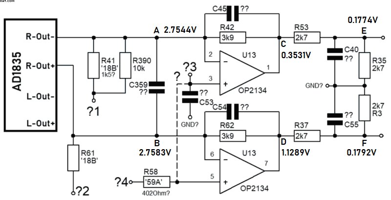
I just pasted the values as shown on my DVM. Value D Seemeilen a bit odd, but was reproducible.
Greetings,
Winfried
I just pasted the values as shown on my DVM. Value D Seemeilen a bit odd, but was reproducible.
Greetings,
Winfried
That's indeed odd, especially as E and F are quite close. Is there some asymmetry further downstream that compensates for the asymmetry caused by R390?
Hi again,
I'll just do it again some time today. The unit was freshly switched on and I've left it on so the electronics are surely settled.
Greetings,
Winfried
I'll just do it again some time today. The unit was freshly switched on and I've left it on so the electronics are surely settled.
Greetings,
Winfried
Node D voltage is impossible unless the output divider resistor is broken (or maybe you have oscillations)
What's the voltage at node 4? That would normally be the 2.7V bias provided by the AD1853.
And the voltage at nodes 1 and 2, is it GND?
The whole circuit looks odd in various regards....
What's the voltage at node 4? That would normally be the 2.7V bias provided by the AD1853.
And the voltage at nodes 1 and 2, is it GND?
The whole circuit looks odd in various regards....
When you look in the first schematic of post #1, you see that one of the outputs E and F is essentially connected to a negative op-amp input that follows the positive input (difference amplifier). Apparently E is connected to the positive input of the difference amplifier op-amp and F to the negative input. That explains why there is only little offset between them.
The offset between C and D can be due to the assymetry caused by R390.
The offset between C and D can be due to the assymetry caused by R390.
@MarcelvdG , I agree with this analysis provided that diffamp is present as per datasheet.
Winfried drew it differently (and most likely not correct).
Winfried drew it differently (and most likely not correct).
@wgh52,
Someone may have already covered the following info. elsewhere in the thread. I confess that I didn't read through every post.
Do you require a differential signal output, or only a balanced interconnection? The two are often conflated, but are not the same thing. Differential drive is a signaling means, while balanced interconnection is a means of rejecting common-mode noise. Jensen Transformers has a good app. note about a simple means of converting an unbalanced output to balanced, I think it's AN003, but I may recall incorrectly. Essentially, it shows an op-amp based unbalanced signal interconnection (such as that via RCA connectors) being made FULLY balanced, simply by adding a very few passive parts. For example, in that application schematic from the AD1853 datasheet, the output interface can be made fully balanced simply by duplicating the existing passive output network. So, duplicate R41, R43 and C50. Call them, say, R41b, R43b and C50b.
Instead of connecting output network R41, R43 and C50 to an RCA jack, connect it to pin-2 of an XLR jack. Connect the duplicate passive network, R41b, R43b and C50b, to XLR jack pin-3. Now, connect the input to R41b to signal ground, not to the op-amp's output. Finally, connect XLR jack pin-1 to the DAC chassis ground. You now have a fully balanced interconnection for the purposes of common-mode noise rejection. The signal drive is still single-ended, while the interconnection is now fully balanced, meaning it enables every dB of CMRR made available by a differentially driven balanced interconnect.
- Home
- Source & Line
- Digital Line Level
- Help requested: DAC I>V conversion, filter, balanced buffer