
I am just getting some parts, the NP FE boards and documentation together to send over to the member in the UK, just in case the original boards are beyond repair.
As you have shown, you have implemented the new NP FE pcb into your stasis amp - and I have not, can you confirm or correct the following as to how to connect the new FE to the Stasis 2 output stage, thanks.
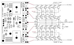
Looking from left to right on the NP FE connections at the bottom of the pcb:
V- = connects to the OS negative voltage rail ( does this wire go to the OS board or PSU caps?
On my stasis, the V- connects to the output stage.
-C = connects to the base of the first transistor marked A6 (PNP) left hand end on the Stasis schematic on the bottom row of 6 output transistors.
I have a different ouput stage on mine but looking at the new and old schematic, That looks like the way you would connect it
-D = connects to the base of the first transistor marked A6 (PNP) left hand end on the Stasis schematic on the second bottom row of 6 output transistors.
Yes, that looks correct
OUT = connects to the pos speaker output connection on the output stage pcb.
Yes
GND = connects to power supply ground - is this on the OS pcb or direct to PSU capacitors?
On mine, there was a thin wire going to the PSU GND
+D = connects to the base of the first transistor marked A8 (NPN) left hand end on the Stasis schematic on the second row from top of 6 output transistors.
That looks correct
+C = connects to the base of the first transistor marked A8 (NPN) left hand end on the Stasis schematic on the top row of 6 output transistors.
That looks correct
V+ = connects to the OS positive voltage rail (does this wire go to the OS board or PSU caps?
On mine, it connected to the v- on the output stage.
Also Nelson has shown a zobel RC on the pcb (R22/10R C6/0.1uF), but I notice that there is one located on the OS board (5R1 / 0.1uF). Did you leave out R22/C6 on the FE pcb?
I don't see any reason why you couldn't use one or the other. Considering Pass redesigned the circuit, it may be benificial to use the new values on the actual front end.
Did you wire in a new 2K NTC thermistor attached to each heat sink, as the original Stasis shows 1K in that position?
I used a 2k. I would try and see how the bias reacts. I tried a 1.5k and the bias circuit did not behave...
Also did you use the existing N/C thermostat (NC thermal breaker on the original Stasis schematic) where it is labelled T on the new FE board?
I actually bypassed this function for a while then evenatually insalled one onto the actual heatsink.
Biasing info would help a lot. what quiescent current (mV across the 1R emitter resistors did you settle on). NP says to adjust till the heastsinks settle at 50 degC ( but at what ambient temp is this for)?
I have a S/500 so the biasing should be different. Stock, the amp had around 70mv accross the 1R resistors.
Keep a close eye on the bias as it warms up. Yes, adjusting until the heatsinks are at 50C is the way to go. The mV of bias will mostly depend on the amount of heatsinking and rail voltage the Stasis 2 has.
I think starting at say 35mv and letting it warm up to see where the temperature ends up is a good starting point. Then increase it by 5 or so mV at a time until you get to 50C. If you are further from your goal, it probably only needs like 15 minutes between adjustments. Once you get within say 5C of your goal, let it rest for a good 30 minutes with the cover on between adjustments.
The only connections that are left are the supplies that went to the A112 and C2592. I suppose these are not used any longer. So instead the 2sc3503 and the 2sa1381 on the new boards are simply getting their power from the rails instead of from the cascodes.
As you have shown, you have implemented the new NP FE pcb into your stasis amp - and I have not, can you confirm or correct the following as to how to connect the new FE to the Stasis 2 output stage, thanks.
Looking from left to right on the NP FE connections at the bottom of the pcb:
V- = connects to the OS negative voltage rail ( does this wire go to the OS board or PSU caps?
On my stasis, the V- connects to the output stage.
-C = connects to the base of the first transistor marked A6 (PNP) left hand end on the Stasis schematic on the bottom row of 6 output transistors.
I have a different ouput stage on mine but looking at the new and old schematic, That looks like the way you would connect it
-D = connects to the base of the first transistor marked A6 (PNP) left hand end on the Stasis schematic on the second bottom row of 6 output transistors.
Yes, that looks correct
OUT = connects to the pos speaker output connection on the output stage pcb.
Yes
GND = connects to power supply ground - is this on the OS pcb or direct to PSU capacitors?
On mine, there was a thin wire going to the PSU GND
+D = connects to the base of the first transistor marked A8 (NPN) left hand end on the Stasis schematic on the second row from top of 6 output transistors.
That looks correct
+C = connects to the base of the first transistor marked A8 (NPN) left hand end on the Stasis schematic on the top row of 6 output transistors.
That looks correct
V+ = connects to the OS positive voltage rail (does this wire go to the OS board or PSU caps?
On mine, it connected to the v- on the output stage.
Also Nelson has shown a zobel RC on the pcb (R22/10R C6/0.1uF), but I notice that there is one located on the OS board (5R1 / 0.1uF). Did you leave out R22/C6 on the FE pcb?
I don't see any reason why you couldn't use one or the other. Considering Pass redesigned the circuit, it may be benificial to use the new values on the actual front end.
Did you wire in a new 2K NTC thermistor attached to each heat sink, as the original Stasis shows 1K in that position?
I used a 2k. I would try and see how the bias reacts. I tried a 1.5k and the bias circuit did not behave...
Also did you use the existing N/C thermostat (NC thermal breaker on the original Stasis schematic) where it is labelled T on the new FE board?
I actually bypassed this function for a while then evenatually insalled one onto the actual heatsink.
Biasing info would help a lot. what quiescent current (mV across the 1R emitter resistors did you settle on). NP says to adjust till the heastsinks settle at 50 degC ( but at what ambient temp is this for)?
I have a S/500 so the biasing should be different. Stock, the amp had around 70mv accross the 1R resistors.
Keep a close eye on the bias as it warms up. Yes, adjusting until the heatsinks are at 50C is the way to go. The mV of bias will mostly depend on the amount of heatsinking and rail voltage the Stasis 2 has.
I think starting at say 35mv and letting it warm up to see where the temperature ends up is a good starting point. Then increase it by 5 or so mV at a time until you get to 50C. If you are further from your goal, it probably only needs like 15 minutes between adjustments. Once you get within say 5C of your goal, let it rest for a good 30 minutes with the cover on between adjustments.
The only connections that are left are the supplies that went to the A112 and C2592. I suppose these are not used any longer. So instead the 2sc3503 and the 2sa1381 on the new boards are simply getting their power from the rails instead of from the cascodes.
Attachments
Thanks Mike. that is how I see it as well, good work on the drawing by the way. In some Threshold info I have on biasing the Stasis 2 says 85mV, but I agree start of lower and gradually increase to the NP 50 deg C HS temp point.
Looks like -D and +D need to connect to the bases of drivers C2592 and A1112 on the output stage to me.
Thanks for that input, I might try and contact Nelson to get him to confirm this for us.
That is what I was wondering. But looking at the picture of TheFinisher's front end from post #62, C2592 and A1112 are on the front stage board. Maybe I am missing something.
Yes I think these are now the C3503/A1381 on the new FE board. So the old C2592/A1112 might be just removed on the OS boards.
I have sent Nelson an email asking to have a look here and advise - hopefully that will sort out the inter connection details for us for a Stasis 2.
I have sent Nelson an email asking to have a look here and advise - hopefully that will sort out the inter connection details for us for a Stasis 2.
On the new FE board, Q7 is the VAS transistor (KSA1381), and Q6 (KSC3503) is the constant current source transistor for the VAS stage.
*edit - looking at this again, I think you are probably correct. The drivers seem to have been omitted due to this more capable VAS in the upgraded FE. I'll return to my regularly scheduled program..
*edit - looking at this again, I think you are probably correct. The drivers seem to have been omitted due to this more capable VAS in the upgraded FE. I'll return to my regularly scheduled program..
Last edited:
paint me simpleton, why bother repairing old one, when new FE is easier and certainly better?
I offered to send the OP a pair of the new and improved FE pcb's, offer still stands..
If you do repair the original driver boards, I reccomend that you replace all of the electrolytic capacitors, and only use caps whigh are rated at 105C. Average cap life is seven to ten years and that's a pretty warm running amplifier, which tends to shorten the life of them. Personally, I'd build Nelson's new design and switch to those.
New updated boards are on their way to me . As I had already ordered replacement caps and resistors for these original boards I thought I may as well try them.
Hi William , I might still need them if I get it wrong with the ones that Gary has sent. I very much appreciate your generous offer mate , very kind .I offered to send the OP a pair of the new and improved FE pcb's, offer still stands..
I know it’s a no brainier really but I had already ordered replacement caps and resistors for the old boards so it’s a case of “ I may as well carry on with repairing them “ as opposed to binning them .paint me simpleton, why bother repairing old one, when new FE is easier and certainly better?
Just replaced the caps and they are all within tolerance , they were not the originals though ( a lifted trace on 2 of them ! )If you do repair the original driver boards, I reccomend that you replace all of the electrolytic capacitors, and only use caps whigh are rated at 105C. Average cap life is seven to ten years and that's a pretty warm running amplifier, which tends to shorten the life of them. Personally, I'd build Nelson's new design and switch to those.
Agree ZM, but in doing all of this the member is learning a lot very quickly. I just need NP to confirm inter connection details with the new NP FE board and the Stasis 2 OS boards.. Maybe you can confirm what post #82 says, thanks.paint me simpleton, why bother repairing old one, when new FE is easier and certainly better?
Once we get all of the details sorted out on what connects to what in the schematic, maybe the next step would be to have TheFinisher take a clear picture of the output stage disconnected from the amplifier with the wires attached to it. With it laying flat on a table with the wires spread out, that should make it easier to sort out all of the connection points.
It may take a bit of time 🙂 Mr Pass is a popular guy...

It may take a bit of time 🙂 Mr Pass is a popular guy...
- Home
- Amplifiers
- Pass Labs
- Help please with my poorly Stasis 2