Good idea Mike with regards to the OS, yeh, hopefully Mr Pass can look at it when he has a chance. We are in no hurry here, the new FE boards are in the mail over to the UK, so that will take a little while.

You are certainly correct on that, replaced with MJ15022/15023 which are good replacements. This looks to me as though it was done some time ago as the ones available are the G types being lead free and these have been around for a few years. The other channel are the original Motorola types - which were 2N5876/5898 types but marked as A6 and A8. You will need to run your meter over them to see if they all compare with similar readings.
Yes, you need a DMM set to resistance range and you go along each transistor and record resistance readings between the 3 pins (B-E, B-C and C-E). So you are comparing all transistors to be roughly the same resistance for the same legs. Bear in mind you may get a resistance reading with the DMM leads one way and if you reverse them you might get open circuit. What you do not want is a short - zero ohm reading on any transistor legs. Record all the readings for reference against each transistor - mark them 1 to 24 with tape or similar so you can identify each one against the resistance checks.
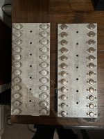
Based on the photos in post #102, the wiring seems to be like this from what I can see:Output parts now removed , left channel appears to have newer transistors fitted
The picture you have shown has the bottom of the output stage assembly at the top of the photo and I see you have marked the heat sink as such. Based on this photo being upside down to the other photo of the rows of transistors my numbering below will refer to the left photo and in brackets to the right photo.
The 12th transistor (top in the right photo) has a blue wire on the base pin (B) on both rows – these are rows 2 and 3 on the schematic.
The 6th transistor (7th from top in the right photo) has an orange wire on the base pin (B) on both rows – these are the top and bottom row on the schematic.
Next, there are yellow wires next to the 6th transistor on either side – these will be the +/- DC supply to the FE board, You will have to double check - the yellow attached to the rail with the 6 off A8 (MJ15022) transistors will be +DC and the yellow wire attached to the rail with the 6 off A6 transistors (MJ15023) will be -DC.
The brown wires attached near the 7th transistor (6 from top in the right photo) will go back to the original FE pcb at the collector (C) of the C2592 transistor and the emitter (E) of the A1112 transistor. Note, these will most likely not be used if you wire in the new NP FE I am sending you ( I am waiting on a reply from NP on this – may take a week or more but he will respond)
This post is to thank Gary .
I really can’t thank him enough actually for how helpful he has/is been.
He has sent me the new revised boards which arrived this morning ( from Australia to uk in a week)
He has also included most of the components for the boards, he has then labelled each component with its value and the location on the board.
He’s also included detailed instructions on the bias settings etc .
I am overwhelmed by the generosity of this man whom I don’t even know ( friends would do less )
Gary you are a legend

No problems, we are here to help, now to get the pcb built and integrated into your Stasis 2.
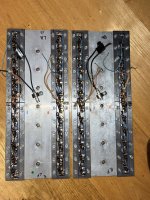
New boards almost completed and shown fitted
Old resistors removed from the output transistors.
I found 3 faulty output transistors on the right channel.
Still to do :
Order new resistors
Order new transistors 2 x mj15022g, 1 x mj15023g .
If I can afford it replace the power supply caps .
Order silicone wires
Figure out ( With Gary’s help) where each wire now goes on the new boards
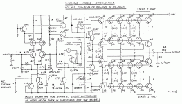
lazy to check where are values for cascode voltage biasing resistors (R23 to R26)
edit, see original schm; so R23=1K, R25=1K5, R26=1K5, R24=1K
use size (power) which Pa implemented in pcb - eyeball - 3W
C9, C10=680pF to 1nF
edit, see original schm; so R23=1K, R25=1K5, R26=1K5, R24=1K
use size (power) which Pa implemented in pcb - eyeball - 3W
C9, C10=680pF to 1nF
Attachments

Last edited:
I didn’t understand a word of that I’m afraid 🤣lazy to check where are values for cascode voltage biasing resistors (R23 to R26)
edit, see original schm; so R23=1K, R25=1K5, R26=1K5, R24=1K
use size (power) which Pa implemented in pcb - eyeball - 3W
C9, C10=680pF to 1nF
But I think you’re saying about the missing components? They’re on their way to me
said resistors and caps - on new FE schematic, those without written values
so, now you have values
though, ask boys - does anyone know ( from original thread) what values are for R27, R28
if you don't know, just put shorts instead
caps C7, C8 - 47uF to 100uF/50V, according to original/old schematioc
so, now you have values
though, ask boys - does anyone know ( from original thread) what values are for R27, R28
if you don't know, just put shorts instead
caps C7, C8 - 47uF to 100uF/50V, according to original/old schematioc
11. What are R25 to R28 values?
Typical 1.5K 3W
I assume that's info from original thread
so, solved
Thanks for your input ZM, and confirmation on the interconnection details. The extra components for the cascade Stasis OS on the new FE were all confirmed to me by NP himself, and are in the original thread for all to see.
For those interested we have been communicating by email and we are making slow progress, bits being gathered to repair existing problems, and new NP FE boards are loaded apart from the 3W resistors that need to be added for the cascade Stasis 2 output stage. I am sure TheFinisher will post updates here as he progresses.
With Gary’s guidance the stasis will be up and running before long , I’ve learned an awful lot over the past few weeks ( my brain did hurt at times 😁 ). There have been many many emails between us , I kind of gave up on the old boards but again I learned a lot from them .
All new parts aside from 12 mj15022’s which I’ve messaged a member about are ordered, they should all arrive in the next week or so .
Now though the excitement of resurrecting the beast is turning into a little bit of worry ( because I simply don’t want to let Gary down after the incredible amount of time he’s given)
I’ve even ordered new power supply caps so the amp almost be as new internally.
Hope I like it !!
You have all been so helpful guys and I am truly humbled by your knowledge and support.
- Home
- Amplifiers
- Pass Labs
- Help please with my poorly Stasis 2