problems return
Well after a period of no problems, the sub amp has come back to haunt me ( could be related to a girlfriend who listens to iggy pop a little too loud 🙁 ).
The obvious cure was to replace the diode that had solved the previous issue. No such luck, I thought perhaps replacing with a higher spec (currently a 5w) zeners in place would fix things. I also replaced the TIP32C to see if this would help.
The sub will fire up and play, however after a relatively short time will crackle become intermittant and stop. If the sub is then turned off for a while the amp will come back on and repeat. All of this a modest volume levels. 😕
First thought is to suspect the LM3886 power IC.
I think we covered most measurements in all this so it is worth checking all the supplies and so on preferably with it in the faulty state.
If the regulated supplies are OK and the rails to the LM3886 OK then I think a new output chip has to be tried as a first step.
Does anything get really noticeably hot ?
You are very patient mooly, but I am a keen student! Ran the sub at moderate volume for about 15 mins, crackle appeared, by dropping the volume I was able to extend the run time before it gave out altogether. The heatsink/plate area was warm but not heated to the level I had expected - I am guessing that you think it is thermal shut down in the IC? There was also heat around the new diode area and regulator transistors, similar to the level of heat above the pins of the chip. I still have the original although my soldering skills make take it's toll on the pcb....
It could be the thermal protection. If the heatsink wasn't as hot as you though then check the IC is in good thermal contact with it. It just sounds like a typical (generalising) symptom of a duff power chip.
As always in faultfinding, all the evidence will be there, so check (to eliminate) that all the supplies are good when it's in the faulty state. That really means measuring on the IC's themselves to eliminate physical board faults etc.
As always in faultfinding, all the evidence will be there, so check (to eliminate) that all the supplies are good when it's in the faulty state. That really means measuring on the IC's themselves to eliminate physical board faults etc.
Progress maybe
35 +/- , the higher of the two in the picture has negligible voltage from it's output to the chip on failure, the lower continues to deliver 35v. The input to the suspected faulty transistor show 35v.
Can you measure the DC voltage at the four points shown and post the results. Make sure the chip doesn't get hot. Do not connect any speaker either.
The two devices ringed look like transistors used as "switches" to control the main power rails to the IC.
You may well find it's one of these and the IC that's the problem.
35 +/- , the higher of the two in the picture has negligible voltage from it's output to the chip on failure, the lower continues to deliver 35v. The input to the suspected faulty transistor show 35v.
Do you mean the higher transistor ?
So in that picture (post #9) you ar saying you have -/+ 35 volts at all times on points 1 and 2 and that point 4 voltage dissapears when faulty while point 3 voltage is still OK ?
If so that indicates the transistor is failing intermitent open circuit (or poor connection).
What transistors have you got fitted in there ?
Yes, TP2 which is a F3055L, TP1 is a D15P05. Point 4 is disappearing on failure, whilst 3 remains good, which I guess ties in with the zener which is on the same track as TP2.
The F3055L is an FET type transistor. Before condeming it check that the two (outer leads) on it are soldered OK. The centre tab will be soldered too. So check all is OK.
If so then measure and record the voltage on the 3 pins. The centre pin is also the tab. Unusual for a FET to fail open circuit but it's possible.
If so then measure and record the voltage on the 3 pins. The centre pin is also the tab. Unusual for a FET to fail open circuit but it's possible.
well if I sneak up on the FET gate, I seem to get 0 volts, however most times when I touch the probe on the gate it will spring back to life and be say 24 or thereabouts. Source showing 35v, drain 0.5 when notworking around 35v when working.
That's still a bit inconclusive as to whether the FET itself is faulty or whether it is a FET drive problem. If the gate were floating then then touching the gate could well give the effect you describe. When it is faulty, does bending the PCB have any effect ?
All you can do is resolder all the area around the FET and the associated components that drive the gate (from the pics I can't make the actual circuit out). If that's still no good then it looks like a new FET has to be tried. I would be tempted to just try a standard leaded part tagged on as a test such as an IRFP240 or even better something like the IRF2907 which has a much lower on resistance but any will work OK. It can be fitted on the top of the PCB by drilling small holes to the print.
All you can do is resolder all the area around the FET and the associated components that drive the gate (from the pics I can't make the actual circuit out). If that's still no good then it looks like a new FET has to be tried. I would be tempted to just try a standard leaded part tagged on as a test such as an IRFP240 or even better something like the IRF2907 which has a much lower on resistance but any will work OK. It can be fitted on the top of the PCB by drilling small holes to the print.
Hmmm , I think I provided incorrect information. This morning during normal operation the gate is around 24v, on stopping it goes to around 32.8v contrary to my readings saying zero. As to the pcb flexing, not really possible, also visual inspection there is no obvious breaks poor connections.
I do not have any fets that I can drop in to assess the problem 🙁
I do not have any fets that I can drop in to assess the problem 🙁
Without a circuit we have to clear on polarities with this.
Looking at the photo's point 2 appears to be the negative rail so should be reading minus 35v ish ?
We have an F3055 FET which is an N channel device. So to turn the FET on we must make the gate more positive than the source by at least 6 or 7 volts.
So that might be a better test. Solder two wires, one to point 2 and the other to the gate and connect your DVM to them reading voltage. So you are reading across the gate and source.
See what the voltage is when the amp is on and then wait and see what happens when the amp fails. See if the gate to source voltage drops or not.
sorry I didn't make this clear. Yes the rail is the negative rail and reading -35v at point 2. and both of the readings in post 112 should be negative. Will post the voltage in the not working stage, but in working mode the voltage is 8.2 positive on the gate and point 2.
8.2 volts across G-S sounds right. If that is maintained when the amp fails then the FET is faulty.
Ok so when not working 0 volts G to S, just to check I have a decent connection the reading then of the Gate to Ground is -32.8 v when not working. Sounds like the FET may be OK?
It does indeed sound like the FET could be OK if the G-S volts drops to zero.
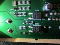
There's nowhere near enough resolution in the pics to see what the circuitry is around there.
My instincts say that it is either one of those tiny SMD transistors failing intermittent open circuit or some physical issue. Have you actually resoldered all those SMD parts in that area ?
Those SMD transistors may be a type that have internal resistors in the base circuit like this,
http://www.datasheetcatalog.org/datasheets/70/194125_DS.pdf
there is PNP equivalent too.
That's only a maybe that they are that type, they may be normal transistors too.
So next step has to be to try and identify at least which are NPN and PNP types and that can be determined by seeing whether the collector (middle lead) is positive with respect to emitter or base. If so we can say it's NPN. If the emitter or base is always higher then the collector then it's a PNP.
As to the fault, again checking base and emitter volt drops is key (like G-S) and seeing if there is any suddenly change, and also seeing if the collector volts on any suddenly changes without a corresponding change in B-E voltage.
I have just stumbled on this thread and read all of it. I have made several LM3886 amps and the info in here might come in useful in the future.
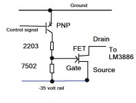
Have a look at this. As best as I can tell from the picture the gate is "pulled" to ground via the path shown. Remember ground is positive with respect to the source on the FET so that gives us the positive voltage needed to turn the FET on.
The resistors are 2203 and 7502. That means 22 and a nought and three noughts giving 220K and the 7502 is 75K. The transistor when on is effectively a short circuit so the two series resistors are across the supply. Ohms law gives a volt drop of around 8.8 volts across the 75K which is the G - S voltage needed to turn the FET on and is what you measured.
So the next test is to see what happens at that small transistor. The base to emitter volts needs to be measured when working. If it's around 0.7 volts and the collector (middle leg) is at zero it's a normal transistor and the amp should be working.
If it's a transistor with the resistors then the base to emitter volts could be anything from say 5 volts upwards. Again this must be measured with the amp working and again the collector will be at zero.
Then see what happens when the fault happens.
So measure and record the voltages on that transistor with the amp working and faulty. Remember if the transistor is PNP the base will go negative with respect to the emitter to turn it on.
Attachments

- Status
- Not open for further replies.
- Home
- Amplifiers
- Chip Amps
- Help noob fix sub amp