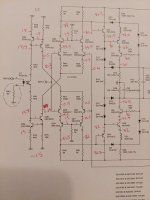
If you're seeing 0.5V at all four resistor pads, the defect must be along the trace that should connect the "ground" pad of R57--- but isn't. Said differently, all four resistor pad show conduction to the base of Q31, so the open has to lie somewhere beyond the ground pad of R57, "north" of the R57 symbol on page 108.
I checked continuity between R57, R58, C28 and pound 1&3 of J1. All good. To make sure J1 digital ground was complete, I installed the amp assy into the case so I was able to install J1. I checked TP4 as a reference and it hasn't changed from the 35V as before.
Looking at the measurements in post #138, I'm curious where the extra 2V comes from at R50 & R51 junction, Q23 collector and Q26 emitter.
Looking at the measurements in post #138, I'm curious where the extra 2V comes from at R50 & R51 junction, Q23 collector and Q26 emitter.
Something still is not correct. Connect black meter lead to speaker ground. Probe path from Q31 base along each pad of R58 and R57 toward the ground pad of R57. If you’re seeing 0.5V, there’s still an erroneous open. There should be only a few mV at Q31 base.
An alternate attack: with power off, measure resistance from Q31 base to speaker ground. Should be 23k, then 22k at junction of R58 and R57, and 0 ohms at ground pad of R57.
An alternate attack: with power off, measure resistance from Q31 base to speaker ground. Should be 23k, then 22k at junction of R58 and R57, and 0 ohms at ground pad of R57.
Last edited:
Then you must be observing 0.5V at ground pad of R57. The problem is open trace or via to ground between R57 pad and earth.
Revisited:
Q31: 0.5V
R58: 0.5V/4.7V
R57: 4.7/ ground side pad is 0.03V
This route:
An alternate attack: with power off, measure resistance from Q31 base to speaker ground. Should be 23k, then 22k at junction of R58 and R57, and 0 ohms at ground pad of R57.
23K and 22K: correct
R57 ground pad measures 6 ohms.
Q31: 0.5V
R58: 0.5V/4.7V
R57: 4.7/ ground side pad is 0.03V
This route:
An alternate attack: with power off, measure resistance from Q31 base to speaker ground. Should be 23k, then 22k at junction of R58 and R57, and 0 ohms at ground pad of R57.
23K and 22K: correct
R57 ground pad measures 6 ohms.
These voltages make more sense, given about 0.5V at base of Q31. It appears you've repaired something along the R57, R58 path, since there are now voltage drops--- in contrast to previous measurements where there none in posts 140 and 144. Can you identify what you repaired? That is, can we be confident that the repair is recognized and will be reliable?
The vexing coincidence(?) is that the bias observed at Q31 base remains at about 0.5V despite a R57,R58 bias string that appears operable. 0.5V/23k is about 22uA which may be a bit high, but may be reasonable if Q28 and Q31 base currents aren't canceling each other.
That you've seen output drop to 35V is at least movement in the right direction. Would you take another look at overall bias:
Output voltage
Q30 base
Q31 base
U3 pin 1
Bias spreader at Q32 collector and emitter.
Thanks again.

Given the measured voltages and the nominal resistor values, I estimate the Q30 base voltage should be about 1.17V. That's lower than what you measure, so I'm not sure what to make of it. With power off and charges bled away, would you measure in-circuit resistance of R56.
If you haven't already done so, I'd recommend getting 10 each of Toshiba-recommended 2SC2713-GR,LF and 2SA1163-GR,LF just to have them available. (a revisit of post 129).
Quite a number of posts back, I believe we had a larger bias spreader voltage than the most recent 1.5V . I'm thinking we should attack the problem from that direction since we're stalled at the front end. I believe that with Q18 and Q6 removed, we had larger spreader voltage. Would you see if that's consistent with your notes ant try to get back to that state?
R56= 276ohm
Q32 with U1 NOT jumped:
BC= 2.5V
CE=3.1V
Q32 jumped:
BC= 0.8V
CE= 1.5V
These are similar to what we got earlier.
Q32 with U1 NOT jumped:
BC= 2.5V
CE=3.1V
Q32 jumped:
BC= 0.8V
CE= 1.5V
These are similar to what we got earlier.
That's a good observation about spreader voltage being larger with U1 not jumped. I regret to confess, I had not noticed that.
I presume Q18 and Q6 are removed. So with U1 not jumped, would you monitor Q32 CE as you decrease R53 resistance? Its voltage should rise smoothly with reducing resistance. Return R53 to max resistance (minimum spreader voltage) to minimize risk to other devices.
With U1 still not jumped, would you report collector voltages at Q36, Q33, emitters of Q38 and Q32.
Then with U1 shorted, please repeat these same voltage measurements.
Thank you.
Hi!
Just to clarify... those measurements were with the unit complete. I haven't removed any components yet.
Just to clarify... those measurements were with the unit complete. I haven't removed any components yet.
FYI, currently I have the amp board assembled to the heatsink. This involves something like 20 bolts and I like having the safety of the heatsink. I can disassemble it for further testing, of course, I just wanted to explain the curve situation.
I appreciate this is a very frustrating exercise for both of us and that you are doing the heavy lifting.
My recommended plan of attack is to "cleave" the amplifier between the Q18/Q6 "front end" and the "back end" with Q18/Q7 and all the power devices that follow. The idea would be to get the entire front end including bias spreader and voltage bias working properly, independently of the output stages. Then we can contemplate how to integrate the output stages with minimal risk.
If you're receptive to this strategy, I'll try to generate details.
Hello again, Happy New Year!
I would love to revisit this, thanks for the offer.
I have now removed the heatsink and put the current limiting resistors in for safety.
I like the idea of separating the front from the back. I plan on measuring every point between the power input and the point where we separated.
Please let me know how you would like proceed. Q6 & Q18, I assume, but anything else?
Take care,
Peter
With the current limit resistors in place, I think it's relative safe to "dive in."
To minimize changes, I suggest disabling drive to the output section by removing base current to either Q6 or Q18. Maybe there's a jumper that could be opened, but removing either transistor is the alternative. The expectation is that all the output devices will be disabled, but that global feedback bias voltage will be maintained from the output via R55 back to the input stage. The output voltage should be about 0V. The bias spreader voltage will be displaced a couple of volts from its normal center voltage because of drops in the transistors, but the spreader should respond to the adjust pot.
I could be overlooking some detail or there may be a defect in the output stages that intervenes, but I think it's low risk to see what presents. Let me know how you elect to disable the drive and what you see.
- Home
- Amplifiers
- Solid State
- Help!!! Dumb-a$$ ham first mistake content