In fact this design is very good, but it does not work by some people because they are not experienced enough in electronics.They think they can simply solder some transistors and resistors together and it will work.It may work for somebody, if he is lucky or not if he is not lucky.And if it does not work they begin to blame the design or the designer.But I think it does not work by some people because they've got bad transistors.Good transistors go to industry and the other, wich are second choice they sell to people like us.
ignore list
BTW, ever heard of an ignore list?
Of course, we are only a bunch of moronic stupid newbies, who don't know what we are talking about. Please accept my sincere apologies for not sharing your excellent insight and far reaching experience in electronics.In fact this design is very good, but it does not work by some people because they are not experienced enough in electronics.
........
BTW, ever heard of an ignore list?
Last edited:
Hi, Edmond
[snip]
Perhaps your question is rather whether the VAS
intrinsical THD is also reduced in the VAS + OPS configuration
when TMC is implemented?
[snip]
cheers,
w
Hi Wahab,
Perhaps we are at cross-purposes. What I meant is that, despite the VAS is part of the TMC loop, the distortion from the VAS is NOT further reduced by using TMC. IOW, no matter TMC or classic Miller compensation, the distortion originated from the VAS will be the same in both cases.
Cheers,
E.
Hi Wahab,
What I meant is that, despite the VAS is part of the TMC loop, the distortion from the VAS is NOT further reduced by using TMC. IOW, no matter TMC or classic Miller compensation, the distortion originated from the VAS will be the same in both cases.
Cheers,
E.
Hi, Edmond
Seems that we did find the common denominator, but we re
still not agree when it comes to its absolute value...
Here a graph that show the single OL vas THD ,
and also the VAS + OPS + TMC config. THD.
We can see that THD is lower in the second case ,
meaning that the VAS THD is indeed reduced by TMC.
Of course, if the OPS is loaded, then producing vast
amounts of distorsions , the reduction in vas THD will be still there
but invisible , as it s masked by the OPS higher THD ratios.
Like wanting to see a little tree hidden by a much bigger one..
Cheers,
w
Attachments
Last edited:
Hi Wahab,
That's weird. I got totally different results. With TMC VAS-THD was only 7% lower.
Cheers,
E.
That's weird. I got totally different results. With TMC VAS-THD was only 7% lower.
Cheers,
E.
Clamp_PM
Hello Edmond
Attached is a file with red X to show where the gain probe should go to do a PM phase margin of the clamp is this correct, with 2V DC at input of amp.
I also added the model of the discrete AD797 circuit for the opamp and compared it to the LME49860 and the THD at 80Vpp 8R 20Khz was 4.5ppm (AD797) as apposed to 4.8ppm THD for LME49860 same condition.
Regards
Arthur
Attachments
Last edited:
Hello Edmond
Attached is a file with red X to show where the gain probe should go to do a PM phase margin of the clamp is this correct, with 2V DC at input of amp.
Hi Arthur,
Yes that's correct and it suffices to look at only the current component. BUT.....
the clamp isn't stable: the ULGF is very high, ~46MHz, and the phase margin is insufficient.

So I had to add a lead-lag compensation, see version 4.
As for the gain probe at the original location, things have changed now, as the output side of the loop has a much lower impedance. This means you have to look at the current and voltage component as well, IOW, use Dr Middlebrook method or so.
If you are lazy (just like me) you can still use the 'current only probe' if you put it elsewhere: at the collector of Q1 respectively Q2, see (and run) the new file.
I also added the model of the discrete AD797 circuit for the opamp and compared it to the LME49860 and the THD at 80Vpp 8R 20Khz was 4.5ppm (AD797) as apposed to 4.8ppm THD for LME49860 same condition.
Regards
Arthur
So, what are your plans, using the AD797 or the LME49860?
BTW, I saw that you have modified R9 & C2 (in your files). Did you have a special reason?
According to my sim, the original values (220R & 390pF) gave a better step response. So I put them back, if you don't mind. 😉
For a better phase margin of the clamp, I've also added R13 & R15. Consequently, I also had to replace the two diode strings by Zeners, as a slightly larger voltage drop was needed (otherwise Q11 resp. Q12 saturated).
Cheers,
E.
Attachments
In fact this design is very good, but it does not work by some people because they are not experienced enough in electronics.They think they can simply solder some transistors and resistors together and it will work.It may work for somebody, if he is lucky or not if he is not lucky.And if it does not work they begin to blame the design or the designer.But I think it does not work by some people because they've got bad transistors.Good transistors go to industry and the other, wich are second choice they sell to people like us.
And we stupid moronic newbies should know that the complementary current mirror circuit leaves no definition of the VAS current in the transfer function and thus will not reliably work with any transistor, even those suposed 'higher' grades claimed by large companies.🙄 BTW, as an individual, I can buy some of the best transistors out there but even the best devices won't solve the problem of and undefined current.

Why should complementary current mirror circuit leaves no definition of the VAS current in the transfer function? Complementary or not, it does not matter.The problem is that if the transistors are not matched in the input stage they will cause a disbalance and this will affect the bias voltage for the cascode VAS.If there were another type of VAS then it would be no such big problem because it would be biased by resistors, but with current mirrors and cascode it's very fine and sensitive.
Extracted from another thread:

I would say follow your own advice!If you want to know what this circuit does, then you can build it in some simulator and test it, but to calculate it is to much work.
I build this amplifier in simulators also.To be precise in proteus VSM and electronics workbench.Worked very well, THD 0.0001 percent and also all other properties good.Good slew rate, no rail sticking and so on.Perfect design.
Hello Edmond
>So, what are your plans, using the AD797 or the LME49860?
My plan is to use the LME49860 because its price to performance is very good, although National also make the LME49990 which has lower THD at higher price and I will try this also. But I must say that the AD797 even after all these years is still the benchmark part for THD +N accept at higher cost. I will be putting down a single opamp footprint
>>BTW, I saw that you have modified R9 & C2 (in your files). Did you have a special reason?
In the download of Pheonix3.cir the original values are R9 &C2 are 490pf and 180R I did not change them but your calculations show otherwise.
>According to my sim, the original values (220R & 390pF) gave a better step response. So I put them back, if you don't mind. 😉
Thanks for changing values
>For a better phase margin of the clamp, I've also added R13 & R15. Consequently, I also had to replace the two diode strings by Zeners, as a slightly larger voltage drop was needed (otherwise Q11 resp. Q12 saturated).
What test do you do test to check that Q11 and Q12 will saturate.
Regards
Arthur
Hello Edmond
...........
What test do you do test to check that Q11 and Q12 will saturate.
Regards
Arthur
Hi Arthur,
Run a trans. analysis of pheonix4 with an input amplitude of ~2.5V or so; fill in Vce(Q11) & Vce(Q12) (or any other tranny that is prone to saturation) in the so called 'Limits Menu' and observe the minimum values. These should be >= 0.5V at any time. That's all.
BTW, You can repeat the analysis for different frequencies. Just go to the 'text page' and define another value for 'ff'.
(please use this file for further developments in order to stay 'synchronized')
Cheers,
E.
PS: I think a LME49860 is good enough, though I wonder, is it 'Alexander friendly', i.e. is it allowed to use the supply pins as signal output. You know that this chip isn't specified for this particular application...............
Alexander Friendly opamps
Hello Edmond
>I think a LME49860 is good enough, though I wonder, is it 'Alexander friendly', i.e. is it allowed to use the supply pins as signal output. You know that this chip isn't specified for this particular application..
Is there any opamp that is specified for the the signal out from the supply pins. I must confess that I had not given it a second thought , and you are right to have some reservations.
Do you think protection you be done next , or the bias generator.
As a rule with protection I include a relay between the amp and speaker to protect the speaker when the amplifier fails , it gets triggered on over current and DC . On top of this I see you like to add additional active output current limiting to protect the output devices , is this your preference.
Regards
Arthur
WOW!
I am glad to see so much of development and inputs on this thread since my last logged in date of 13th July.
All this while I have been totally enjoying this amp through high sensitivity speakers and HF titanium compression drivers.
The transistors I am using are not quality ones which I purchased locally but I will upgrade to the best in my next holiday season from OnSemi. It still performes well!
Sharing Notes: In one channel I am stuck with BD139 for simple VAS and I removed the harshness by increasing the input sensitivity and was “JUST” able to reducing the CDOM by 10pf (to 90pf & 90pf). Consequence; slight hiss at compression driver. Since the OP transistors are slow devices I got some surprises when I used high FT devices in driver stage. Since I ran out of time I had to stick with this gross adjustment.
Advice:
Hi Oliver! if it works at one time and not the next, then it could be oscillations when load is not tied up properly with OPS, then drivers could induce oscillations on the OPS. (Keeping it short on track or cable inductance & capacitance).
I have used highly matched device on IP and VAS
I am eagerly waiting for my next break when I will read this tread in detail and share some of my tweaking skills with various components.
You guys really rock!
Best regards,
smathias
Hello Edmond
>I think a LME49860 is good enough, though I wonder, is it 'Alexander friendly', i.e. is it allowed to use the supply pins as signal output. You know that this chip isn't specified for this particular application..
Is there any opamp that is specified for the the signal out from the supply pins. I must confess that I had not given it a second thought , and you are right to have some reservations.
Hi Arthur,
I'm not aware of any op-amp that is specified for this kind of application. But I do know that someone has dropped a list of 'Alexander friendly' op-amps on this form, but where?
Do you think protection you be done next , or the bias generator.
Yes, that's my next step.
As a rule with protection I include a relay between the amp and speaker to protect the speaker when the amplifier fails , it gets triggered on over current and DC . On top of this I see you like to add additional active output current limiting to protect the output devices , is this your preference.
Regards
Arthur
Sure, that's a good idea. Speakers as well as the OPS must be protected.
Hello Edmond
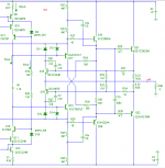
Here is my attempt at the amp with output protection.
Regards
Arthur
I'm sorry Arthur, but that doesn't work correctly. It's far more complicated. For this kind of protection, the VAS needs a current limiter too.
Before I go on with this stuff and the bias generator, what about multiple output devices and/or thermal track trannies?
I the meantime I've modified the driver stage. Now it's a diamond buffer with bootstrapped collectors of the pre-drivers, so the VAS doesn't see Cob. As a result, the distortion is about half as low.
Also the thermal compensation can be made simpler now. Pre-driver and main-driver compensates each other (if thermally coupled, of course). So we have only to deal with the compensation of the output devices.
What do you think about it?
Cheers,
E.
edit: The zero load THD20 dropped from 2.7 to 0.5pmm 🙂
Attachments
Last edited:
Output Device Protection
Hello Edmond
>I'm sorry Arthur, but that doesn't work correctly. It's far more complicated. For this kind of protection, the VAS needs a current limiter too.
I like your approach it represents a very complete solution. I have attached my take but is short of the compensation on the Q15 and Q16 (your circuit values).
>Before I go on with this stuff and the bias generator, what about multiple output devices and/or thermal track trannies?
The reason I always build an amp around a single pair of Sanken outputs (2SC2922/ 2SA1216) is because they are the most powerful pair of transistors you can get for the real estate they use. They have a use where lots of channels of audio power amps are needed, and a space restraint.
Secondly where higher power and lower distortion into low impedence loads is needed by all means I go for lots of output devices and I have no problem with Thermal Track transistors.
I like the way the diamond buffer has two benefits simplifying thermal compensation and reducing further the non linear capacitance the VAS stage sees . I have always wanted to do this between the VAS and the output devices but I never got around to it.
With MC9 what capacitance variable do you graph to show less Loading from Cob with a diamond buffer.
To progress it would be nice just to finish the single pair amp, and then go to multiple pair output amp could the same temperature compensation for both amps or is there something else at play, like amplifier stability.
One other thing the THD of the amplifier very low , for an amp of this complexity and PCB area its excellent, this input stage is state of the art .
Regards
Arthur
Attachments
- Home
- Amplifiers
- Solid State
- HEEEELLLPPP : M. Randy Slone Mirror Image Topology Construction - Troubles