Hi Arthur,
The values of the freq. comp. components are cc9 = 1nF & rc9 = 56R.
BTW, they don't compensate Q16/16, rather Q22/23.
As for the OPS, only one pair and still +/- 63V and a load of 4 Ohms? I'm afraid the SOA will be quickly exceeded under these conditions, unless you lower the supply voltages.
Even with +/- 50V I would opt for two pairs.
Regarding the temp. compensation, it's a bit tricky with this design. The point is that the loading on the VAS output should be kept as low as possible. Even a small capacitance of 10pF has already an effect on the performance. Now imagine what a classical Vbe multiplier will do, a TO126 tranny that is mounted on the heat sink...... Right!
Also, we have issues with the thermal delay.
I think that a design as advanced as the Phoenix deserves a more sophisticated thermal compensation, IOW, the ThermalTraks from ON. Admittedly, the power-handling capability of the NJL4281/4302 is not as good as the Sankens, but it comes quite close.
One more point: What about starting a new thread, as the Phoenix project has little to do with the original subject of this thread, i.e. solving issues with the Slone amp.
Cheers,
E.
PS: For your info, I've attached the complete schematic of the new clamps (plus TMC and and two pairs in the OPS, if you don't mind)
Attachments
Pheonix Project
Hello Edmond
>One more point: What about starting a new thread, as the Phoenix project has little to do with the original subject of this thread, i.e. solving issues with the Slone amp.
I will start a new thread and if you don't mind what do you think I should call the new thread be called.
Regards
Arthur
Well, actually it's your project, so you have to decide. But what do you think about:
"Rebirth of the Phoenix"? (admittedly, rather obvious and not quite original)
Cheers,
E.
"Rebirth of the Phoenix"? (admittedly, rather obvious and not quite original)
Cheers,
E.
The phoenix thread is indeed continued on the afore mentioned link but the actual thread of making Slone's design work and make further optimisations is continued here. I will soon post the circuit as I have it for the moment here again...
Greetz to All
Olivier
Greetz to All
Olivier
Modified Mirror Image (Slone) still not working !!!
Hello all,
Yesterday I fired up my latest trial of making Slone's mirror image topology (with beta enhancers / current mirrors / cascodes / ...) work.
As we all know, the basic schematic is not working due to the ill defined VAS Iq.
For this I followed the idea of Edmond Stuart (CMCL). He copies the VAS leg and creates a feedback to the Input Stage to correct for the DC instability.
Secondly the TPC is removed and replaced by TMC to avoid signal overshoot.
Result :
On the DC side the circuit seems quite stable. No more frying Q's or class C operation with the slightest temperature change....
The problem now seems to be on the AC part :
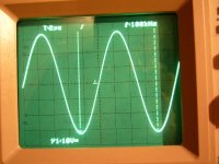
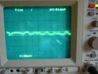
I am stuck with an ugly sine wave of 10VDCpp (the sine wave looks like it is mixed with a 2nd and/or 3rd harmonic of herself) most of the time at 1,5Mhz (but sometimes it is half the freq and sometimes double the freq). Note : the trace is most of the time very clear. I mean it looks sharp on the scope and it remains triggered (so it is not random high freq noise).
While my VAS Iq is calculated at 7mA it seems to be only 3,4mA ... other DC voltages and currents seem correct ...
I still didn't search deeply into it (since i just powered it up yesterday night) but I hope connect to you guys to start a troubleshooting ...
I will post schematic soon ...
Thnx
Olivier
Hello all,
Yesterday I fired up my latest trial of making Slone's mirror image topology (with beta enhancers / current mirrors / cascodes / ...) work.
As we all know, the basic schematic is not working due to the ill defined VAS Iq.
For this I followed the idea of Edmond Stuart (CMCL). He copies the VAS leg and creates a feedback to the Input Stage to correct for the DC instability.
Secondly the TPC is removed and replaced by TMC to avoid signal overshoot.
Result :
On the DC side the circuit seems quite stable. No more frying Q's or class C operation with the slightest temperature change....
The problem now seems to be on the AC part :
I am stuck with an ugly sine wave of 10VDCpp (the sine wave looks like it is mixed with a 2nd and/or 3rd harmonic of herself) most of the time at 1,5Mhz (but sometimes it is half the freq and sometimes double the freq). Note : the trace is most of the time very clear. I mean it looks sharp on the scope and it remains triggered (so it is not random high freq noise).
While my VAS Iq is calculated at 7mA it seems to be only 3,4mA ... other DC voltages and currents seem correct ...
I still didn't search deeply into it (since i just powered it up yesterday night) but I hope connect to you guys to start a troubleshooting ...
I will post schematic soon ...
Thnx
Olivier
Update
Too bad for me no-one seems to be interested in this problem...
Anyway, there is some progress. I had to fiddle with the ground wiring of the thing. I made many different ground points.
1 for positive DC return line
1 for negative DC return line (these first two are cabled together)
1 for input ground together with feedbackground
1 for common ground which is also connected to a midlayer1 kopper plane
1 for top layer shield. I poured full copper on the islands between tracks
1 for midlayer2 shield
1 for bottomlayer shield
I guess it were better to separate the signal GNd for input and feedback. Is this necessary or very facultative?
I am not sure weather using shields is good and how to connect them? Maybe one shield is better than shields on multiple layers...
What works best for now =
DC return GND + and - together with top and bottom shield (i don't like this because it will bring DC return GND rubbisch onto my shields no?)
The midlayer2 shield is best not connected in my case.
Common GND separatley.
All these connections go to the middle connection of the powersupply. If I connect this middle point to the powersupply GND or not is in some case better and in some cases not. Mostly it doesn't change much.
The input/feedback GND is connected to the GND of the scope and to the GND of the signalgenerator.
I removed the TMC too because I cannot juge it's behavior and will put it back when everything else works.
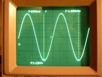
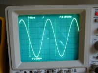
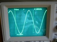
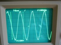
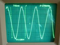
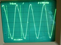
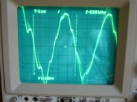
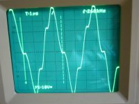
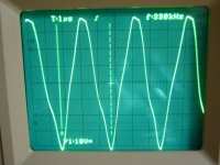
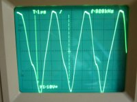
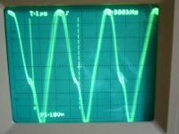
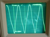
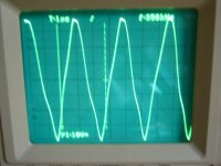
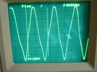
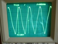
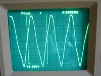
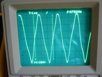
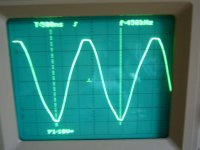
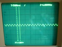
I have a nice sine up 147KHz. But then at 148KHz it suddenly changes form. There is a higher freq sitting on it with 10% of amplitude of sine wave. This is quite much. I guess this higher freq is roughly 5 times higher thus 750KHz. It is mostly only visible on the negative cycle and not on the positive cycle.
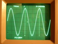
Going further into freq over 150KHZ the wave looks still the same. At 250KHZ it starts to drop in amp since we crossed the CL HF fall-off freq.
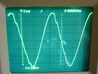
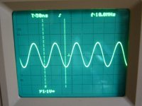
As we continue the dirty wave becomes better again (is this because the 5fth order freq riding on it now goes over the unity gain of the amp?). It looks better because there is no high order freq riding on it anymore but it starts to go to a triangle wave as freq increases.
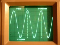
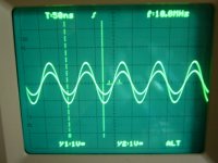
Once we arive at 850KHZ (we are stil way below unity gain freq - is modeled to be at 20MHZ - is too high i guess) the signal dissapears and is replaced by RF oscillations.
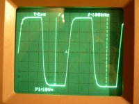
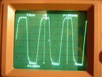
The square wave follows the same behavior. Even if this is diffucult to measure for me i noticed the slewrate is near 60V/us.
What am i dealing with here?
Is this clear talk to anyone?
any hints?
Thnx
I will post schematic tomorrow and pictures too ...
Thnx
Too bad for me no-one seems to be interested in this problem...
Anyway, there is some progress. I had to fiddle with the ground wiring of the thing. I made many different ground points.
1 for positive DC return line
1 for negative DC return line (these first two are cabled together)
1 for input ground together with feedbackground
1 for common ground which is also connected to a midlayer1 kopper plane
1 for top layer shield. I poured full copper on the islands between tracks
1 for midlayer2 shield
1 for bottomlayer shield
I guess it were better to separate the signal GNd for input and feedback. Is this necessary or very facultative?
I am not sure weather using shields is good and how to connect them? Maybe one shield is better than shields on multiple layers...
What works best for now =
DC return GND + and - together with top and bottom shield (i don't like this because it will bring DC return GND rubbisch onto my shields no?)
The midlayer2 shield is best not connected in my case.
Common GND separatley.
All these connections go to the middle connection of the powersupply. If I connect this middle point to the powersupply GND or not is in some case better and in some cases not. Mostly it doesn't change much.
The input/feedback GND is connected to the GND of the scope and to the GND of the signalgenerator.
I removed the TMC too because I cannot juge it's behavior and will put it back when everything else works.
I have a nice sine up 147KHz. But then at 148KHz it suddenly changes form. There is a higher freq sitting on it with 10% of amplitude of sine wave. This is quite much. I guess this higher freq is roughly 5 times higher thus 750KHz. It is mostly only visible on the negative cycle and not on the positive cycle.
Going further into freq over 150KHZ the wave looks still the same. At 250KHZ it starts to drop in amp since we crossed the CL HF fall-off freq.
As we continue the dirty wave becomes better again (is this because the 5fth order freq riding on it now goes over the unity gain of the amp?). It looks better because there is no high order freq riding on it anymore but it starts to go to a triangle wave as freq increases.
Once we arive at 850KHZ (we are stil way below unity gain freq - is modeled to be at 20MHZ - is too high i guess) the signal dissapears and is replaced by RF oscillations.
The square wave follows the same behavior. Even if this is diffucult to measure for me i noticed the slewrate is near 60V/us.
What am i dealing with here?
Is this clear talk to anyone?
any hints?
Thnx
I will post schematic tomorrow and pictures too ...
Thnx
Is this clear talk to anyone?
any hints?
Thnx
I will post schematic tomorrow and pictures too ...
Great, a schematic would be very helpful to answer to theses questions...
Hi Wahab,
I will post schematics, pictures of the pcb, scope trace pictures, etc... this evening (that is GMT+1 evening) but most probably it will be tomorrow.
Thnx already...
Olivier
I will post schematics, pictures of the pcb, scope trace pictures, etc... this evening (that is GMT+1 evening) but most probably it will be tomorrow.
Thnx already...
Olivier
Hello,
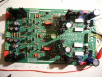
Here are the files of my latest trial... with only limited succes i must say.
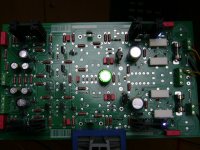
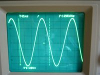
The files contain the schematic, dc analyses for currents & voltages, the AC analyses, some pictures of the PCB and some pictures of the scope image.
The schematic & pcb do not contain any OPS yet. The VAS output is returned to the IS via the feedback layout.
First of all, looking at the AC analyses I don't like the bandwidth to be so large. Especially in the HF region. But trying to bring it lower I end up with millercaps nearing 1nF !? That seems outrageously large. This will suffocate my IS right?
If you look at the AC analyses bear in mind the black line is the one OUTPUT/INPUT at the base of diff amps. The green one is the ratio between the BASES of the diff amps feedback side and the BASES of the diff amp input side. The red one is output / input source (off course this one looks nice because the low and high freq rolloffs are set by the input conditionning circuit. But anyway the BLACK one is the internal one ... (i don't know if the green one is of any value?)
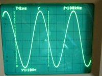
Secondly I find it odd that the output signal suddenly at 149KHZ changes from looking good to looking bad AND mostly on the negative side not on the positive side or much less. Why? What causes this behavior?
As I said in my previous mail you can read just above ... at 850KHZ or so the trace goes into RF oscillation I guess... just buzzing and bouncing around
Maybe you guys can do something with the square behavior ... see pictures too....
Please I need help as my knowledge is alas limited ... I know the basics and a bit more but I am not a wizard like some of you ...
Lets what you guys come up with?
rest of the pics in the next post
thnx
Olivier
Here are the files of my latest trial... with only limited succes i must say.
The files contain the schematic, dc analyses for currents & voltages, the AC analyses, some pictures of the PCB and some pictures of the scope image.
The schematic & pcb do not contain any OPS yet. The VAS output is returned to the IS via the feedback layout.
First of all, looking at the AC analyses I don't like the bandwidth to be so large. Especially in the HF region. But trying to bring it lower I end up with millercaps nearing 1nF !? That seems outrageously large. This will suffocate my IS right?
If you look at the AC analyses bear in mind the black line is the one OUTPUT/INPUT at the base of diff amps. The green one is the ratio between the BASES of the diff amps feedback side and the BASES of the diff amp input side. The red one is output / input source (off course this one looks nice because the low and high freq rolloffs are set by the input conditionning circuit. But anyway the BLACK one is the internal one ... (i don't know if the green one is of any value?)
Secondly I find it odd that the output signal suddenly at 149KHZ changes from looking good to looking bad AND mostly on the negative side not on the positive side or much less. Why? What causes this behavior?
As I said in my previous mail you can read just above ... at 850KHZ or so the trace goes into RF oscillation I guess... just buzzing and bouncing around
Maybe you guys can do something with the square behavior ... see pictures too....
Please I need help as my knowledge is alas limited ... I know the basics and a bit more but I am not a wizard like some of you ...
Lets what you guys come up with?
rest of the pics in the next post
thnx
Olivier
Attachments
-
IS and VAS AC analyses.pdf122.9 KB · Views: 130
-
IS and VAS DC analyses currents.pdf26.9 KB · Views: 103
-
IS and VAS DC analyses voltages.pdf23.5 KB · Views: 123
-
IS and VAS schematic.pdf20.6 KB · Views: 192
-
 PCB1.JPG91.1 KB · Views: 281
 -
 PCB2.JPG94.6 KB · Views: 268
 -
 100KHZ_BLOK.JPG97.6 KB · Views: 239
 -
 1KHZ_SINUS.JPG96.6 KB · Views: 237
 -
 1KHZ_BLOK.JPG98 KB · Views: 248
 -
 100KHZ_SINUS.JPG98.5 KB · Views: 115

Hello.
As I can see it beginns to be unstable at 150kHz.But I think it's not a big problem because audio signals are going only to 20kHz.With an input filter should be no problem.And You set your current sources for 6.25mA.I think it's too much.Try to reduce it and see what happens.I think 4mA is a good value to beginn with.
As I can see it beginns to be unstable at 150kHz.But I think it's not a big problem because audio signals are going only to 20kHz.With an input filter should be no problem.And You set your current sources for 6.25mA.I think it's too much.Try to reduce it and see what happens.I think 4mA is a good value to beginn with.
Last edited:
update
Hi there,
Since the last post there are some updates.
Hereby the schematc as it is built right now (after further testing).
What changed?
1) I removed the input HF filter capacitor Cin2 because I wanted to measure the AC response of the amp without the filter up front. I worried this would render it unstable since i allow VHF injections at the input. I was affraid it picked up RF noise.... but no it doesn't.
2) I reinserted the TMC compensation instead of a single miller cap. While this was not realy the intention it is there now because I soldered and unsoldered so many times so many components to check the behavior. Maybe I will remove it again soon to go back to a single miller cap (when i do i will let it know)
3) What helped quite a bit was removing R105, R106, C101 and C102. I don't know their purpose very well? It is part of the CMCL so it should be DC related only. While it does not change anything to my DC settings it made the amp less vulnerable to RF oscillations. If the have no important purpose I would rather skip them (but then again I ignore their purpose so.. anyone could tell? The caps are quite big 470nF so I gues it's lpow freq related?
4) I removed cap C900 & C901 it did not change anything as far as i can notice....
5) CFB2 is reduced from 10pF to 5,6pF ... I don't really know if this chnged much because often one probleme covers another and nested errors lead you to believe it doesn't change a thing while at that moment it is not because a bigger phenomen is lying on top swamping it's behavior ...
6)CFB1 is set to 470u instead of 3x times this value because i soldered only 1 cap instead of three however this is only impacting on the LF rolloff point tight?
7)My QCC1&2 are replaced by another type since I blew the last two ... It is now type : 2SC5171 & 2SA1930. They are slightly higher power Q's but have a bit more Cap and a bit lower FT. For the rest I guess it's not critical since they are just cascodes.
I send the schematic as it is build here in front of me ....
Also AC analyses,DC voltages and currents...
+ pictures of
-> output without input
-> pcb topview
-> 100KHZ sinewave
-> picture of each increment of 10kHz and further on larger steps.
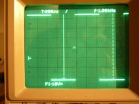
-> Up until 10MHz maximum for my function generator.
-> Last picture = at 10MHz input and output signal. Output is stil twice the input signal or +6dB amplified.
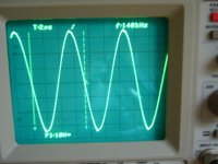
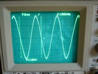
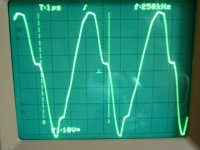
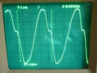
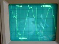
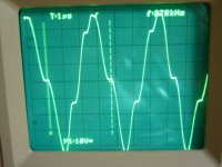
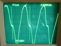
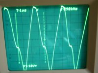
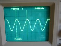
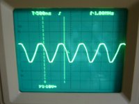
What do you see?
I see good respo,nse till around 130KHZ where the sinewave starts to show bumps in the curve. This gets worse till a point around 250-300KHZ where the trace also starts to become shaky showing oscillations (RF?) ... afterwards the sinewave looks more and more to a sine again over 1MHz it is nearly a perfect sine -> look at 10MHZ it looks a perfect sine (why??)
My 2 major curiosities are :
A) the sudden bumps in the trace at 130KHZ why so sudden? It is a bump but it looks clear on the scope I mean it's not shakyness ... Why is that.???
B) The shakiness at 250-300KHZ i guess here it is an internal stability issue somewhere in the schematic / pcb .... but why does it go away further up the freq?
OK I gotta go now ... wife is already waiting in the car 😉😉😉
She : 😡
Ideas?
Olivier
Hi there,
Since the last post there are some updates.
Hereby the schematc as it is built right now (after further testing).
What changed?
1) I removed the input HF filter capacitor Cin2 because I wanted to measure the AC response of the amp without the filter up front. I worried this would render it unstable since i allow VHF injections at the input. I was affraid it picked up RF noise.... but no it doesn't.
2) I reinserted the TMC compensation instead of a single miller cap. While this was not realy the intention it is there now because I soldered and unsoldered so many times so many components to check the behavior. Maybe I will remove it again soon to go back to a single miller cap (when i do i will let it know)
3) What helped quite a bit was removing R105, R106, C101 and C102. I don't know their purpose very well? It is part of the CMCL so it should be DC related only. While it does not change anything to my DC settings it made the amp less vulnerable to RF oscillations. If the have no important purpose I would rather skip them (but then again I ignore their purpose so.. anyone could tell? The caps are quite big 470nF so I gues it's lpow freq related?
4) I removed cap C900 & C901 it did not change anything as far as i can notice....
5) CFB2 is reduced from 10pF to 5,6pF ... I don't really know if this chnged much because often one probleme covers another and nested errors lead you to believe it doesn't change a thing while at that moment it is not because a bigger phenomen is lying on top swamping it's behavior ...
6)CFB1 is set to 470u instead of 3x times this value because i soldered only 1 cap instead of three however this is only impacting on the LF rolloff point tight?
7)My QCC1&2 are replaced by another type since I blew the last two ... It is now type : 2SC5171 & 2SA1930. They are slightly higher power Q's but have a bit more Cap and a bit lower FT. For the rest I guess it's not critical since they are just cascodes.
I send the schematic as it is build here in front of me ....
Also AC analyses,DC voltages and currents...
+ pictures of
-> output without input
-> pcb topview
-> 100KHZ sinewave
-> picture of each increment of 10kHz and further on larger steps.
-> Up until 10MHz maximum for my function generator.
-> Last picture = at 10MHz input and output signal. Output is stil twice the input signal or +6dB amplified.
What do you see?
I see good respo,nse till around 130KHZ where the sinewave starts to show bumps in the curve. This gets worse till a point around 250-300KHZ where the trace also starts to become shaky showing oscillations (RF?) ... afterwards the sinewave looks more and more to a sine again over 1MHz it is nearly a perfect sine -> look at 10MHZ it looks a perfect sine (why??)
My 2 major curiosities are :
A) the sudden bumps in the trace at 130KHZ why so sudden? It is a bump but it looks clear on the scope I mean it's not shakyness ... Why is that.???
B) The shakiness at 250-300KHZ i guess here it is an internal stability issue somewhere in the schematic / pcb .... but why does it go away further up the freq?
OK I gotta go now ... wife is already waiting in the car 😉😉😉
She : 😡
Ideas?
Olivier
Attachments
update (followed)
the pictures
the pictures
Attachments

update (followed2)
...
...
Attachments

update (followed3)
...
...
Attachments
- Home
- Amplifiers
- Solid State
- HEEEELLLPPP : M. Randy Slone Mirror Image Topology Construction - Troubles