This way or another, Vref impedance is more than high enough. More important, it's stiff and ripple free - MOSFET's gate doesnt draw current and BJT's Ib is miniscule (hfe is very high).
I regularly use polymer caps (Murata, NIC, Chemicon...), but here the Low ESR is more important. Sometimes it makes a sonic difference, sometimes not. Open another cap thread and we'll discuss it at length...
I regularly use polymer caps (Murata, NIC, Chemicon...), but here the Low ESR is more important. Sometimes it makes a sonic difference, sometimes not. Open another cap thread and we'll discuss it at length...
The low ESR of the organic polymer caps was the reason for the suggestion🙂, but your right, is is for a different thread.
My progress and a few questions
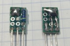
Hi Juma, I managed to get started on this project yesterday, and made the two adapter PCB with BF862 (pic attached). Not so pretty perhaps, but it works. Both has Idss of 13,2x at 10Vds. The big blobs of solder at the top is not a mistake: I thought it would make a nice heatsink for the gate pin.
Was going to start on the main PCB today, but can see you have made some adjustments to the design again (in post 37):
1. Minor changes in resistor values, and film cap bypass across output cap.
2. Lowpass (RC) filter added on the +40V supply.
- Is this just for good measure, or did you actually have some noise problems?
Do you happen to have a schematic (or picture of) for the power supply you use now? Would like to see exactly how it looks.
3. Q4 is now a BC547C instead of BC546B (was called Q1 in your previous version from post 24).
- So a higher gain device. Is this an important change?
I have BC550C and BC546B in stock (and SC2547E, but not sure they are genuine), will any of these work instead (as good)?
Thanks 🙂
Attachments
Another thought: Is the hFE of the Bipolar devices critical? Should they be matched, and if so, at what value?..
Hi jvhb,
R13, R12 changed - sounds a bit better this way to me (sch. from post #37).
RC filter (10R, 22uF) used for channel power decoupling - same power supply used for both channels.
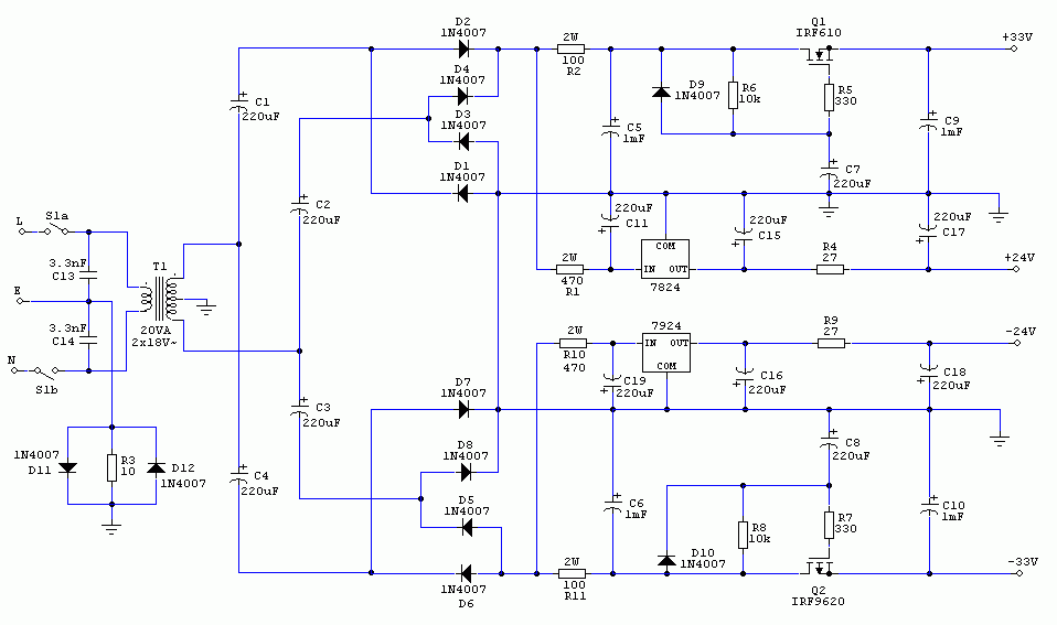
I can't draw schematic now but the PS is very simple - 36V ac/10 VA power transformer, four UF4007 diode bridge, 1000uF/63V cap to GND, 220R/O.5W in series, 1000uF/63V cap to GND followed by simple cap multiplier with irf610 - like this one (used in +33V rail), cap values are not critical - 220 to 470uF is OK:
http://www.diyaudio.com/forums/atta...4110-lsk-pre-baf-2013-lsk-baf2013-psu-sch.gif
BC550C is great - higher hfe means lower Ib i.e. stiffer Base Vref but BC546B sounded a tiny bit better on higher output levels (5V or so) when I used this pre to drive LATFET power buffer.
Strict matching of transistors is not needed.
R13, R12 changed - sounds a bit better this way to me (sch. from post #37).
RC filter (10R, 22uF) used for channel power decoupling - same power supply used for both channels.
I can't draw schematic now but the PS is very simple - 36V ac/10 VA power transformer, four UF4007 diode bridge, 1000uF/63V cap to GND, 220R/O.5W in series, 1000uF/63V cap to GND followed by simple cap multiplier with irf610 - like this one (used in +33V rail), cap values are not critical - 220 to 470uF is OK:
http://www.diyaudio.com/forums/atta...4110-lsk-pre-baf-2013-lsk-baf2013-psu-sch.gif
BC550C is great - higher hfe means lower Ib i.e. stiffer Base Vref but BC546B sounded a tiny bit better on higher output levels (5V or so) when I used this pre to drive LATFET power buffer.
Strict matching of transistors is not needed.
BC550C is great - higher hfe means lower Ib i.e. stiffer Base Vref but BC546B sounded a tiny bit better on higher output levels (5V or so) when I used this pre to drive LATFET power buffer.
Ok, so the choice is mostly subjective, and all of the mentioned BC fets will work well. The 550 has lower noise (on paper at least). But I assume you now prefer the 547C to the 546B and 550C, since you changed to the 547C in latest published schematic? Or do you still swap them around, and try to hear any differences?
Are yours Fairchild devices? The ones I have now are CDIL, so I might get different results.. Will get some Fairchild from Mouser soon.
Regarding PS: So you are not using Zener regulation now?
BCanything... it's just a simple cascode - not that important... There are very small differences and I often use BC547C in sch as generic type and BC550C in the real build and the difference between the two in this circuit is not worth mentioning because very critical listening is needed to even tell if there is a difference at all...
BF862 is a critical part, good caps are needed too (not cheap chinese junk), build everything nicely and the rest is trivial...
Why would i need zeners ? Couple of volts up or down is not important here. Voltage ratios are important, but not the precise value of ps voltage.
BF862 is a critical part, good caps are needed too (not cheap chinese junk), build everything nicely and the rest is trivial...
Why would i need zeners ? Couple of volts up or down is not important here. Voltage ratios are important, but not the precise value of ps voltage.
Last edited:
Hi Juma, I asked about Zener regulation, because earlier in this thread you gave the impression you were using that in your PS.
(...)3 x 15V zeners connected in series, from gate to ground and a 5mA CCS from drain to gate to feed the zeners. That gives about +41V at the source pin..
I took them out since the zeners eat additional 5-7ma with no real benefit. But if you prefer stiff supply voltage, it's OK - no real damage too...
Hi Juma, thanks for clearing that up.
Two questions regarding resistors, if you have time:
1. The Base resistor for BJT: Should this be 220 or 470 with a BC550C? (I have seen both values on your schematic)
2. R4 and R9 which you have on the RCA connectors: Any reason not to mount them on the PCB instead?
Two questions regarding resistors, if you have time:
1. The Base resistor for BJT: Should this be 220 or 470 with a BC550C? (I have seen both values on your schematic)
2. R4 and R9 which you have on the RCA connectors: Any reason not to mount them on the PCB instead?
Hi jvhb,
1. Doesn't really matter, use what you got in that range
2. Mount them any way you like
1. Doesn't really matter, use what you got in that range
2. Mount them any way you like
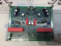
Perf-board build done. Some problems..
Hello, not much activity here I see 🙂
Well I finally got around to building this pre-amp. I thought it would be simple to do on a perf/prototype board, but it actually took me quite a while to get right. Will make (or order) a PCB next time I think..
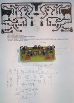
I followed the schematic and instructions from post #37 (also attached here).
Only two minor differences from the schematic:
For the resistors on the output, I have used 22 for R9 (instead of 18), and 33k for R4 (Instead of 27k).
The good news is that both channels worked first time, so I didn't make any critical errors in the point-to-point wiring.
Gain is x5,2 with 100mV input.
The BF862 both have Idss=13,2mA
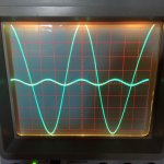
Bad news is that both channels do have a problem:
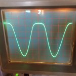
When the input signal gets above 300mVpp, the positive waveform looses amplitude - looks like a very soft clipping.
Please see attached pics for example of this. At 1,41Vpp input, the positive half of the waveform is clearly flattened on the top.
Both channels give the exact same result!
The preamp is getting a stable 40V dc from a lab PSU (varying the supply voltage from 25-45V doesn't affect the issue)
Test signal is 1Khz Sine from HP339A.
I have a feeling there is a simple explanation for this, I just can't seem to find it.
Has anyone seen this before?
Hello, not much activity here I see 🙂
Well I finally got around to building this pre-amp. I thought it would be simple to do on a perf/prototype board, but it actually took me quite a while to get right. Will make (or order) a PCB next time I think..
I followed the schematic and instructions from post #37 (also attached here).
Only two minor differences from the schematic:
For the resistors on the output, I have used 22 for R9 (instead of 18), and 33k for R4 (Instead of 27k).
The good news is that both channels worked first time, so I didn't make any critical errors in the point-to-point wiring.
Gain is x5,2 with 100mV input.
The BF862 both have Idss=13,2mA
Bad news is that both channels do have a problem:
When the input signal gets above 300mVpp, the positive waveform looses amplitude - looks like a very soft clipping.
Please see attached pics for example of this. At 1,41Vpp input, the positive half of the waveform is clearly flattened on the top.
Both channels give the exact same result!
The preamp is getting a stable 40V dc from a lab PSU (varying the supply voltage from 25-45V doesn't affect the issue)
Test signal is 1Khz Sine from HP339A.
I have a feeling there is a simple explanation for this, I just can't seem to find it.
Has anyone seen this before?
Attachments
jvhb,
please measure and report the following voltages :
1. across the R2 (4R7) - should be about 50-60mV
2. across the R8 (47R) - should be about 500-600mV
3. between the source of Q6 (BS170) and the GND - should be about 27V
4. between the base of Q4 (bc547c or bc550c ) and the GND - should be about 13.5V
5. the Vgs of Q6 - should be about 2.3 V
6. the Vbe of Q4 - should be 650-700 mV
7. across R12 (680R) - should be about 7.5V
8. across R1 (10R) - should be 100-120 mV
Last edited:
Hello juma. Thank's for the quick reply.
I have just checked both channels, and the one that really jumps out is #3: I have 37,2V instead of 27V. The Vgs of Q6 is also reading high at 2.6V.
Here are the results (almost identical between both channels):
1. 50mV
2. 504mV
3. 37,2V (!)
4. 13.9V
5. 2.6V (!)
6. 555mV (?)
7. 7,3V
8. 108mV
So does that mean the BS170 are the problem?
Seems unlikely that they should both have the same fault.
>Edit: Just noticed that the Q4 Vbe is reading low. I am using BC550.
Last edited:
The source of bs170 is at too high voltage and that's why you hit the rail too soon (early clipping).
The node where R22, R21 and R23 meet the + pole of C4 should be at about 30V (ref. to GND) but I suppose it is at almost rail voltage, so check the value of R22 out of the circuit - it should be 68k (68000 Ohms) - if that's OK, then your Q4 is no good. BS170 is OK.
Edit: bc550 is not recommended -it should be bc550C - high hfe.
Also check other resistors for values as per schematic (out of circuit of course).
Last edited:
Yes I have over 36V on that node where R21, R22 and R23 meet.
I have just pulled one of the BC550C (yes they are C type), and it shows hfe of 600 on my (cheap) transistor tester. So they seem just fine, but they are CDIL devices and not Fairchild. Perhaps they are inferior somehow?..
I don't have any other high gain devices around - only lower hfe.
The R22 are indeed 68K, have just checked them again.
I can't practically check all resistors out of circuit - that is of course a problem with p2p building/soldering. But I double checked and matched all values before I started, so have high confidence in the resistors being correct. And when I measure them in circuit, I get readings very close to the schematic values. Only the 100k seem tricky to measure in circuit - they read more like 50-60k. But I know for sure they were 100K before installing them.
So the reason for the problem still seems uncertain somehow.
Guess I will try and buy some Fairchild BC550C, and see it that helps.
>> Edit: Problem is solved! I went back and rechecked the connections accroding to the schematic, and found I had soldered R21 to the top of R22, instead of to the bottom node. I had made the same mistake on both channels. Now it measures correctly, and output is looking good. More testing, and also listening will follow.. 🙂
Thanks again for your help.
Last edited:
That bc550c looks OK.
If all components values are OK too, then it must be some node connection problem (or maybe leaking caps).
Check everything against the schematic once more...
If all components values are OK too, then it must be some node connection problem (or maybe leaking caps).
Check everything against the schematic once more...
Succes
After i fixed the error with R21, output is looking very good. The risks of p2p soldering I think, but it was an easy fix at least. Sorry I didn't spot it earlier.
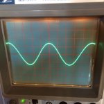
Here is a shot of 1 Khz sine 0,3Vrms input. My HP339A reads 0,25% THD, and the distortion residual shape is textbook 2nd harmonics. Nice 🙂
After i fixed the error with R21, output is looking very good. The risks of p2p soldering I think, but it was an easy fix at least. Sorry I didn't spot it earlier.
Here is a shot of 1 Khz sine 0,3Vrms input. My HP339A reads 0,25% THD, and the distortion residual shape is textbook 2nd harmonics. Nice 🙂
Attachments
What was the error with R21 - wrong value or wrong connection ?After i fixed the error with R21,...
That's too much of second harmonic you got. Try lowering the R2 to 2R2 (to raise the current through the circuit) or use the BF862 with higher Idss (say 16 mA or so). Also experiment with the value of R13 (3k3 - 10k) and see what you get - distortion should be much lower (for an order of magnitude at least).My HP339A reads 0,25% THD, and the distortion residual shape is textbook 2nd harmonics. Nice 🙂
I had soldered R21 to the top of R22, instead of to the bottom node - same mistake on both channels.
Thanks for your suggestions, I have just tried some different values in these positions:
- Lowering R2 to 2R2 did not help, actually the THD increased very slightly.
- R13: I first held a resistor in parallel to get around 3K2, and the THD dropped visibly, to around half. So I tried going even lower, to 2K5, which lowered the THD further to 0,088% at 0,3V input (at higher V input, the THD is also higher - nearly 1% with 1V in). So this did reduce THD substantially, but not by an order of magnitude, and it also reduced the gain to x3. In addition, at lower input levels, eg. 0,1V, the distortion doesn't look good now: it has lost the 2nd harmonic base, and is just completely mixed.
Done for today now, but will perhaps try a higher value (over 4k7) in R13 tomorrow..
- Home
- Amplifiers
- Pass Labs
- Gyrator loaded Son of ZV9/F3