Hi Eldam,@ Ryan,
I've done a picture though I didn't want to draw it ! On the picture there is twice the same idea but the left shematic is focused (zoom !).
Nice drawing 😀
The way you've drawn the current returns for pins1-4 isn't quite right. Its not a very easy thing to visualise. The currents will follow the path of least impedance, which will be as close as possible to the equal but opposite charge. This means directly under the traces and directly under the center of the chip. This is why i made the PCB 1.2mm instead of 1.6mm thick - to make impedance matching easier. A 1.6mm PCB would have meant the need for thicker traces (pin 1-4) which would have meant more compromises. If the plane is separated this way the impedance will be many times what it is now, it may make a nice antenna though 😛
On the other hand I know this DAC isn't operating very high in the MHz, but the rising and falling edge of the square waves would be in the Ghz (not sure) if they were a sine wave.
Thanks for the links to where the discussion all started, good to read over it again. 🙂
Ryan
Hi ryanj,Hi Walter,
Thanks for reminding me, I'm very keen on having a play with attenuating the I2S/PCM. Ill have to have a look at some designs/ideas. I remember seeing it on ECdesigns thread somewhere... Got a link? Or as simple as a series resistor and another resistor going to ground?
The only reason it wasn't included is because i've never experimented with this at all. A few years ago I made up a PCB that used Johns I2S reclocking/attenuation circuit but never ended up populating it... Must have got sidetracked, doesn't take much. 😀
Do you mean this one?
http://www.diyaudio.com/forums/digital-line-level/79452-building-ultimate-nos-dac-using-tda1541a-434.html#post3029991
I2S attenuation
I think in John's frustrated attempt for perfection, several evolutions were provided. I think post #5029 is the last presented. http://www.diyaudio.com/forums/digi...e-nos-dac-using-tda1541a-503.html#post3922229
I note that my original ARCAM board just used a single series resistor. I checked values - 380R in series. Circuit is shown on lampizator site, search Arcam http://lampizator.eu/LAMPIZATOR/TDA1541 corner/TDA1541.html
I think that sometimes 80% of the gain might come from the simple approach. I would be tempted to experiment with the simple series resistor and see if there is a perceptable improvement. Also, if I read it correctly, looks like a simple series diode might do the trick?
Last edited:
yes remembered that ! Ryan wanted to stay on a simple design about I2Sinput but also clocking schemes. The only few things which were added with my asking is the simultanous way and uf-l pads and maybe also Andrea Mori and I with vias holes for an MCLK. And don't forget the signal diodes attenuation needs a sort of 3D design as each I2S signal lines needs 3 signal diodes in serie iirc John's writtings !
Ryan found after some experimentation the 6K8 resistors (with an older pcb) around the dem sync cap à la John gave a better result alone than with BCK or LE injection and btw it seems John himself just uses the simple 6k8 resistors in the latest designs without any capsfor RC filter and clock injection circuit with it!
Some versatile choices are hard too choose sometimes as they introduces also some problems with RF (my simple understanding) : difficult to add as I asked zero ohms jumper on cutted traces with hole vias also on the trace to put the three diodes signals in serie John advised for the jitter attenuation like the traces for caps to do a sot of RC filter : as you can see the Distinction-1541 is very tiny and I can remember Ryan wanted to make it under controll choosing the simpliest way : If you followed this thread of the common development we tried it was a real pain to have common decisions and also fight against some hassoles and bad willings minds 😉 At the defense of Ryan : we made what we could and it was complicate enough. Maybe we had to follow more the advices of T. Loesch and I remind some member like Audiolapdance to insist on this with legitim reason !
But I can assure you it was not an easy task to share and involve everybody as the egos are huge here. But Ryan had a good willing to share what he begann before and add what some suggest on this pcb and even if it's not as good as a T. Loesh or P. Rogic design due to some groundloop issue and some versatility (it's a test pcb after all), Distinction is certainly better than all the Ebaykits made behind the kitchen....😀.
Don't forgett it's RF and one can have a huge knowledge, experience and great tools to do a top pcb... Distinction-1541 is the result of a versatility where you can choose the input stage as the output one with a core pcb around the final DAC... and for sure there is some limitations because that... but it stays imho better than the others EbayKit !
What to do for a V2 :
-read again T. Loesch & John ECDESIGNS. Understand what is writted between the lines as well.
-Involve more top RF ingineer members like Marce and some others
-Experiment with beta pcbs to choose some final choice against some others
-A more talentuous people than I am with my bad english to involve the good willed members to help (a big thanks again to all the members who helped for the Distinction design) and fight against the bad faithed ones and some ******** !
I tryed to ask for a DIY contribution to members to give money and time to Ryan but without sucess !
Difficult job guys than to developp together something though we had a certain sucess with the Distinction-1541 pcb : for the one like me who has one : you can understand it in relation to the crappy Ebay pcbs !
I'm sure Ryan will listen to all the good ideas but here the hardest to find is some common time to share togethers and even alone for the drawer: time consuming task !🙁
Don't forgett as well some member like CFT (Cheung from HK) asked to Audial and we have an re edition of the AYA-2 for few money to support the DIY cause with some new things Pedja added with him open mind : uf-l connectors. I have one and I am totaly pleased with it !
cheers
Eldam
Last edited:
I2S attenuation
Ryanj
One other reference. I looked at the circuit diagram for Acko's S03 reclocker board. He places a 22r series thin film resistor in the trace immediately after the ufl input connector on each of the I2S traces.
digikey part A103067CT-ND 22R 0603 THIN FILM RES.
So it looks like many different approaches from 20r/390r/500r have been employed.
It could be a nice option in your next run of the PCB to simply put a set of pads that people could put an in series attenuator of choice, or simply a copper bridge.
A second suggestion would be to see if there is room on the first 2 MSB decoupling caps for the next size up, so that a 1u film cap could be placed there without going on its side.
Only problem is if you do all these things, I'll have to buy another one to try it out🙂
Hi Wloves,
better zero ohms smt resistors than different coper piece ! If it could help :
those low values you spoke about are often here to avoid reflexion on the I2S lines before the emitter and the receptor (the dac chip); here the value is not thinked about the jitter itself.
If it helps (?) John used with the TDA1541 3x signal diodes in serie instead a resistor for each I2S line. You can also re ask on the John thread what is the value and ref of the diodes : was it used in reverse position ? can't remember and mostly I'm not technician at all 🙁)
Unluckilly have not the link. But in the "Any good TDA1541 kit" , T. Loesch (aka Mr T.) in the beginning of the thread copied a shematic. But this shematic was simplified by John himself later, of course in him thread. Though most of the Distinction came from him inputs and some final choices but trying to stay versatile (choice between smt resistor and caps like bulk ones, simultaneous mode or nor, etc !)
The better is to read the long thread of the Ultimate TDA1541 DAC by John but beginn the reading at approximatly 4/5 or 2/3 if more time to do it.
But also, keep in mind P. Rogic as T. Loesch don't use this I2S attenuation. I surmise you have more to gain elswhere (6072 tube as Mr T. uses it 🙂 30 years of experience with tda1541 and tubes; he uses russian tubes but with some others dac chip at AMR : 1305 e.g. with the DV-777 but not with TDA1541 and the cd-77 flag ship... though he tried it! )
At least I'm sure your is really good enough and remind me I have to do my own casing as well ...
Hi Walter, Damien.
There are just a few things to consider if attempting to attenuate Digital transmission lines.
Slowing down Rise time on BCK through the use of a resistor or diode will cause deterministic jitter. Impedance matching is really important which is why i used a program to calculate this. I think further circuitry is required if this was to be attempted. Simulation and experimentation is definitely required here. (resistor to gnd as well as the series resistor for example). Its critical stuff.
Ackos resistors in series may have been for impedance matching.
I also wonder whether the gains to be had will be worth the hassle. Keep in mind if your using simultaneous data input, BCK is shut down for 75% of the sample period, which is probably why having Ians i2s to pcm pcb sounds that much better. ECDesigns had the same findings.
In my opinion, further gains that are easier to obtain should be considered. Such as:
A lower phase noise XO. The crystek 957s are ok as are the NDK ones used in the Waveio. Andreas solution looks like it might perform well with the Laptech crystal. The Pulsar clock has impressive phase noise performance : -90dBc @ 1Hz for 11.2896MHz. Some good reviews from people who have compared it against the Crystek. If you can get one of Jockos clocks... but he hates us diyers...
Other very easy gains (and cheaper) by the use of better cables, an LDR volume attenuator. I experienced this yesterday when i had Jame Hill (jameshillj) over for a listening session. Opened my eyes to other areas where simpler gains can be had. Lets not forget about room treatment - Diffusers and absorbers.
Diminishing returns attenuating Digital lines? - Yeah I think so. Theoretically it should reduce noise within the DAC thus reducing jitter, but, with Ians i2s to pcm board you are getting 75% less noise anyway.
Ryan
Hello Ryan,
I totally agree : not really worth it and add length to the I2S layout! Though I find the idea of Walter has interrest: maybe checking the need of a smt resistor near each input pin of the I2S in serie in the case it's needed is not so hard and there are excellent low noise smt resistor with close spec in precision and with low noise).
But maybe better to focus on the Clock work : Ian, Andrea Mori, hopping the ground layout to be good enough. Many Distinction are on service and work 🙂.
I2StoPCM from Ian :double yes ! Have it on the AYA2 and find it better ! Despite a limited budget, I decided to go for the FIFO... I sold my DAM1021 R2R and keep the money for the Ian's V2 clock board + FIFO 2 and still hoping the clock from ANDREA very close to the DGND and the other pin and device involved for the I2S will add some improvement (despite those multi board in the RF domain... TDA1541 is not a ES9018 100 Mhz... even if Ian have done some positiv test with such Fs and reclocking)
Better if a V2 to re-think from scratch the ground circuit design (maybe staying with the analog ground star though John swaped finally on the lateral DEM caps positions à la Pedja & Thorsten and from so many else... maybe not without reasons ! I don't know. Post 360 and furthers ?
We talk no too much of the output stages... Mine when time and money will be for tubes. As already said, having the AYA2 2014, its outpustage is certainly hard to challenge with a discrete ones !
Ryanj
Sounds like you have thought this through very well. As I said in the beginning, I was just looking for your thoughts on this and see best gains to be had now in the source of my I2S signal and its timing.
I used the Lightspeed for years and remain an advocate. Last year I replaced it with Dave Slagle's autoformers which left Lightspeed in the dust. If you want a boost, I highly recommend skipping over Lightspeed and go straight to AVC.
Eldam, so your planned setup will be wavio ----> fifo ----> XO ----> i2S_PCM ----> Distinction then tube I/V? Will you use Shanes stage? The design is not entirely clear to me , but I expect others here can fill in the gaps, ie what ccs to use and what current.
Wlowes, thanks for the ebay link, I should probably make a wooden bobbin if I make these, sounds like fun.
Wlowes, thanks for the ebay link, I should probably make a wooden bobbin if I make these, sounds like fun.
Noise on analog outputs with simultaneous data input.
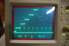
Hey guys,
Been playing around with the scope to try and capture what's going on with the noise being put out at the analog outputs(Top trace). I played a 1k sine wave (16/44.1) at full current swing; just because i already had it on the computer. You can clearly see what's going on. Have a look at each sample when BCK(bottom trace) is pulsing. There is clearly more noise at the last 25% of the sample. This explains why the i2s to pcm board is clearly an improvement.
Walter, yes gave it a lot of thought, we may only be chasing a very minor improvement, but its good to keep a conversation ticking over. Keeps it interesting. Ill check out that attenuator you mentioned.
Cheers
Attachments
Last edited:
ryanj,
I second Slagle avc, have both, the clarity and musicality of the avc leaves the ldr in the dust, spend the extra, you won't be disappointed.
Laters,
Drew.
I second Slagle avc, have both, the clarity and musicality of the avc leaves the ldr in the dust, spend the extra, you won't be disappointed.
Laters,
Drew.
Hi Luke,
Yes exactly this one. I will try also between the Wave I/O isolator and the one Ian provided nicely as a gift in its last shippment.
To me there are some pain in this way, not talking of the cost : big interconnect length (4" uf-l wires between each board), many low noise regs and traffos (EMC !).
I asked to Ian if it can source 2" uf-l wires and makes plug connector which are compatible with Wave I/O or Amareno also to improve the sheilding and return path of each I2S line. He always listen the askings of diyers, test it and if he can : keep it. Ian is a serious guy.
Of course I would like he makes in a standalone board : usb or tcpip input+isolator+fifo+clock+simultaneous 😀... FIFO is better very close to the inputs pins of the DAC I surmise (to avoid a new jitter between the FIFO and the dac chip due to a too long path on the boards - in this regards the little I2S length traces of the Distinction1541 are welcome- like the uf-l wires between the last board and the dac board). But we also putted two holes for a MCLK stacked right above the dac chip: Andrea's way !
The best would be connectors plugs below the pcb at the edge to plug/stack on the edge of the next pcb (to avoid length when possible) :
it could be only by a same designer : here Ian... and as it's the best we can have today it's a good news 🙂.
The uf-l plugs for the Distinction1541 were mostly asked for Ian and Wave I/O, DIYhinkh, products which allows uf-l plugs on their own boards!
We certainly don't want to waste all those good designs with bad interconnects !
Last edited:
Drew, Walter.
Interesting concept, hard to believe it could sound better than a Warp speed or the like. Still uses those sliding ladder type contacts? Whats the advantage exactly? Betting impedance balance? I read that you can get a small amount of gain out of setups like this? (1.25dB)
Interesting concept, hard to believe it could sound better than a Warp speed or the like. Still uses those sliding ladder type contacts? Whats the advantage exactly? Betting impedance balance? I read that you can get a small amount of gain out of setups like this? (1.25dB)
Ryanj,
As far as Iunderstand the signal is tapped off a single winding, so the load to the output(dac) never changes, just the signal level to the next stage is changed, makes the load consistent and therefore more linear.
I may be wrong, just how I understand it, as you can see, there are a couple of wires to hook up.......
Laters,
Drew.
- Status
- Not open for further replies.
- Home
- Source & Line
- Digital Line Level
- Group buy/Interest list - TDA1541A Core board.