Hi, I'm in with schematic first , later I will layout PCB .🙂
Alex.
Go to it , alex !!! 🙂🙂 sigh of relief. You are 1 step ahead of me in layout "magic" 🙂
OS
Hello Par,
I would like and support you 🙂 !
I sold my old DX AMP several weeks ago and will contribute its returns (it is not much: 34.50€) into parts needed for the one (Keantoken?) who will prototype this AMP.
Send me a PM once you have received Keantoken's order list.
Best regards - Rudi_Ratlos
I would like and support you 🙂 !
I sold my old DX AMP several weeks ago and will contribute its returns (it is not much: 34.50€) into parts needed for the one (Keantoken?) who will prototype this AMP.
Send me a PM once you have received Keantoken's order list.
Best regards - Rudi_Ratlos
Last edited:
Hahahahahahahahahahaha, someone made me laugh and smile this sunday morning!!! 😀 🙂I sold my...and will contribute its returns into parts...
By the way, nice to see alexx mm around, and I like small form factor.
no worries rudi. ill keep you updated once i get the list from keantoken!
lets make sure we get this done! 😉
lets make sure we get this done! 😉
Hello Par,
I would like and support you 🙂 !
I sold my old DX AMP several weeks ago and will contribute its returns (it is not much: 34.50€) into parts needed for the one (Keantoken?) who will prototype this AMP.
Send me a PM once you have received Keantoken's order list.
Best regards - Rudi_Ratlos
Question to Alex and Kean.
Were we supposed to have four pairs of outputs and do we really need drivers since the vas is buffered? How abuut a small resisistor in series with R12 to prevent accidents. Just asking.
Jam
Were we supposed to have four pairs of outputs and do we really need drivers since the vas is buffered? How abuut a small resisistor in series with R12 to prevent accidents. Just asking.
Jam
+-80Vdc across the outputs.
What impedance loads are you expecting to drive?
4pair seems about right for severe reactance 8ohm and 6ohm speakers and probably about right for moderate reactance 4ohm speakers.
Drivers for FET output stages. Read Cordell.
Yes, 51r in series with 100VR would limit maximum Tail current to ~12mA.
What impedance loads are you expecting to drive?
4pair seems about right for severe reactance 8ohm and 6ohm speakers and probably about right for moderate reactance 4ohm speakers.
Drivers for FET output stages. Read Cordell.
Yes, 51r in series with 100VR would limit maximum Tail current to ~12mA.
Last edited:
So are you saying there's nothing wrong with it?
BTW, could someone please check these gerber exports? I need to know if the way I'm using the PCB software makes any sense...
- keantoken
Hi Kean
I had a look at your gerbers.
There are some issues with it:
Silkscreen covers pads. Some board houses offer to remove this for you but in some cases there won't be much left of the print.
For the bottom layer you generated a file named back and another named group2. Back only includes pads, group 2 pads and copper. I don't know what's the intention behind.
File names.
Front and Back aren't recommended.
Use top an bot instead, label top and bot in copper letters, only bot mirrored so that you can read it on final board.
Soldermask top
Soldermask bot
Silkscreen top
board outline
plated drill is okay
You have a lot of clearance issues.
Maybe you like to add some thermal reliefs to pads connected to copper planes.
Good luck.
Lee
Yes to the 4 outputs per side, for a total of 8🙂!!!
And YES to including the shunts on the board too. Is there a FINAL close schematic available for that?
Is there a REGULAR regulator NEEDED to feed the shunts, if so THEN which one?
Can we put the TMC(Transitional Miller Compensation) on the board as a Option?
Lets give ALEX as little grief as possible... IF you have a suggestion or want to be address, PLEASE do it up front, so it can be decided on EARLY in the game. Rules are needed to avoid conflict down the line.
Thanks again to ALL kibitzers, commentators and contributors ETC.
Lets BRAND this project with a NAME....
I vote for GOLDIYA1 😀
Thanks
Lets BRAND this project with a NAME....
I vote for GOLDIYA1 😀
Thanks
Nice name suggestion, like some capricious diva Lady 😉
Looking the keantoken's schematics only one comment I have: let's omit R36 & R39 220 ohm collector resistors and rather put VAS load resistors app. 10-22 kohm from emitters Q13 & Q14 to ground to linearized VAS load impedance and thus even more lower frequency dependent distortions. 🙂
Nice to see the thread burst into life again. Kean, I suggest you appoint two enthusiasts to build and tweak the prototypes so that the community gets feed back from two separate sources. The builders should have access to test equipment as well, not only golden ears.
I concur with Lee that you have issues with spacing between tracks and track widths, your PCB layout program should have a facility that allows to check the Gerbers for such issues automatically.
Kind regards.
Nico
I concur with Lee that you have issues with spacing between tracks and track widths, your PCB layout program should have a facility that allows to check the Gerbers for such issues automatically.
Kind regards.
Nico
since the original is goldmund, ie gold mouth and since i like to thumb my nose atit perhaps goldschnauze (gold nose) is a good name...?
Hi, I'm in with schematic first , later I will layout PCB .🙂
Alex.
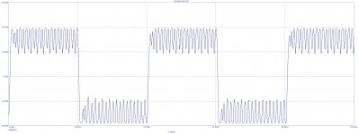
Running a simulation on the schematic of post 1037, attached are square wave and phase responses into 8 ohm resistive load. Is this intended or is there an error in the schematic?
Kind regards
Nico
Attachments
since the original is goldmund, ie gold mouth and since i like to thumb my nose atit perhaps goldschnauze (gold nose) is a good name...?
ahem, never mind. someone who speaks german (as opposed to my google translate) shared that this word isnt a very nice word... so scratch that!
Running a simulation on the schematic of post 1037, attached are square wave and phase responses into 8 ohm resistive load. Is this intended or is there an error in the schematic?
Kind regards
Nico
Did you NOT get the 411 on this project...

We are building a sinusoidal based square wave generator...😛😀
Thanks
does 411 mean something in the States?Did you NOT get the 411 on this project...:
does 411 mean something in the States?
Telephone directory assistance - 411
- Home
- Amplifiers
- Solid State
- Goldmund Mods, Improvements, Stability