Well I got it together, but using a trimmer for R5 was a bad idea this time. It is hard to adjust. I don't have any more time but I will replace it with a fixed resistor and use a trimmer for R1.
There was also a lot of subsonic noise resembling triangulated pulses, which I'm thinking is either trimmer noise (which explains the LF noise I observed earlier which seemed less than random), or perhaps it's the 6.3V 100uF cap giving fits from being reverse biased the wrong way around on first startup. I've never dealt with either of these issues before, but I'll have to figure it out tomorrow.
- keantoken
The way to have choice on the number of output devices will be to have a board that is narrow and will allow for break off or non usage. The original design by Alex for the "other" board I think is best in it's configuration. I will diagram it up to day.
Just as Kean has actually BUILT some circuitry. We need to BUILD some amplifier circuitry.
Lets get this show on the road. I am not at all envious of the Other side but would like to show SOME progress, which we are but it is not to obvious to the causal observer.
Thanks
Just as Kean has actually BUILT some circuitry. We need to BUILD some amplifier circuitry.
Lets get this show on the road. I am not at all envious of the Other side but would like to show SOME progress, which we are but it is not to obvious to the causal observer.
Thanks
the Other side
Which one is the Dark side?

By the way, we are looking forward to watch the results from both projects!
Congratulations for the efforts.
Max.
Which one is the Dark side?
By the way, we are looking forward to watch the results from both projects!
Congratulations for the efforts.
Max.
Salas, do you think it would be possible, if one wants to use FETs for the shunt, do directly replace BJTs and resistors without needing to change the board layout?
It seems OS will soon build something very close to what we have here.
Aside from that, I wonder if someone could whip up a dead-bug style ground plane prototype? How hard can it be?
- keantoken
It seems OS will soon build something very close to what we have here.
Aside from that, I wonder if someone could whip up a dead-bug style ground plane prototype? How hard can it be?
- keantoken
Aside from that, I wonder if someone could whip up a dead-bug style ground plane prototype? How hard can it be?
- keantoken
would it make sense to have ground plane for frontend only
and use both sides around the output for whats needed there only
btw, have you left the option with seperate boards for frontend and output ?
Salas, do you think it would be possible, if one wants to use FETs for the shunt, do directly replace BJTs and resistors without needing to change the board layout?
It seems OS will soon build something very close to what we have here.
- keantoken
It happens in my LV V1.0 vice versa, in this one here you got to simulate for Mosfet subs and check the closed loop phase margin will be adequate before attempting it. Compatible pin order BJTs to Mosfets should be examined.
OS must be having some low pinch off low IDSS Jfets to check out in its Vref too?
What if we stacked the frontend board vertically on top of the power board? Perhaps this could work well with a ground plane between the two.
- keantoken
- keantoken
The reg has been set at 5.0045V. It has since drifted about 50mV after several minutes to warm up. 50mV*18=900mV drift at 90V.
Simulation seems to indicate that 1.2k is the best value for R1 for most BJTs, except that most models don't model Beta tempco IIRC, I will have to check.
I readjusted it a few minutes ago, and it seems to be staying within 30mV.
- keantoken
Simulation seems to indicate that 1.2k is the best value for R1 for most BJTs, except that most models don't model Beta tempco IIRC, I will have to check.
I readjusted it a few minutes ago, and it seems to be staying within 30mV.
- keantoken
Is that close enough for government work? You know, MIL Spec.
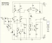
Please update the schmo and show details of ALL critical parts that affect board layout. I should be close on it.
What is the VA on that transformer?
Thanks
Please update the schmo and show details of ALL critical parts that affect board layout. I should be close on it.
What is the VA on that transformer?
Thanks
Theoretically, I should be able to get it be constant within 11mV at 5V, which is about 200mV at 90V.
Unless you intend to prototype this, I would go with the older "final" schematic that I posted. It should be good enough.
- keantoken
Unless you intend to prototype this, I would go with the older "final" schematic that I posted. It should be good enough.
- keantoken
YES, we WILL build test and verify independently ALL aspects, then NO arguments and premature ejacXXXX assumptions and such.
Lets build one somewhere and then layout a board to be compatible with the rest of our system and then on to the real deal.
Thanks and lets make this open for kibitzing all round...
Also what is the residual drift on your voltage meter?
Lets build one somewhere and then layout a board to be compatible with the rest of our system and then on to the real deal.
Thanks and lets make this open for kibitzing all round...
Also what is the residual drift on your voltage meter?
Last edited:
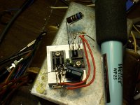
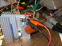
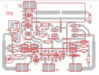
Here is some pics of how I laid it out. The only long wires are the CCS collector (Q1) and the negative power wire. I stacked the TO92's face down on the TO126's (the TO92 2SC945's have ECB pinout, which is convenient this way). Q4 can be any TO92, hopefully not something preposterous (this one had EBC pinout). At 90V Q2 should be a TO126, and should be Vbe matched with Q5. (referring to the schematic in post 816).
To adjust:
Set R5 to 10k. Adjust R1 for lowest tempco, or lowest difference between idle and startup voltages. Then increase R5 to the desired output voltage.
Salas, can you elaborate on how to choose and adjust the Jfet version?
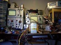
My meter shows 4.997V, with the 5th place wandering. It has wandered +-50mV in the time I have observed it, excepting startup where it was several hundred mV higher. This means I should increase R1. I don't know how much of the wandering comes from CCS fluctuations, or from the 100uF cap doing weird things, or (quite possibly) the trimmer I'm using for R1. In any case, noise above 100Hz is below 10uV for the 5V version, and will I think be the same for the 90V version.
Noise increasing below 100Hz is predicted by the simulator, if this is due to CCS variations. I may try a MOSFET CCS to see if this is so. (at 100mA, Ib of Q1 is near 1mA, and Vce/Early effect will vary this greatly)
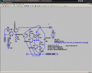
Attached is a schematic of how I would lay the design out optimally. If you are measuring output impedance or pulse response, measure from the top of C1 and the bottom of C3.
- keantoken
To adjust:
Set R5 to 10k. Adjust R1 for lowest tempco, or lowest difference between idle and startup voltages. Then increase R5 to the desired output voltage.
Salas, can you elaborate on how to choose and adjust the Jfet version?
My meter shows 4.997V, with the 5th place wandering. It has wandered +-50mV in the time I have observed it, excepting startup where it was several hundred mV higher. This means I should increase R1. I don't know how much of the wandering comes from CCS fluctuations, or from the 100uF cap doing weird things, or (quite possibly) the trimmer I'm using for R1. In any case, noise above 100Hz is below 10uV for the 5V version, and will I think be the same for the 90V version.
Noise increasing below 100Hz is predicted by the simulator, if this is due to CCS variations. I may try a MOSFET CCS to see if this is so. (at 100mA, Ib of Q1 is near 1mA, and Vce/Early effect will vary this greatly)
Attached is a schematic of how I would lay the design out optimally. If you are measuring output impedance or pulse response, measure from the top of C1 and the bottom of C3.
- keantoken
Attachments
Salas, can you elaborate on how to choose and adjust the Jfet version?
- keantoken
Right Kean. Well, if someone wants to use a Jfet current source for creating a full output voltage reference drop on R5 in your schematic (connected as shown in the previous pages circuits you posted), has to get some low pinch off low IDSS part for better regulation and ability to work under just Vbe potential. Examples are J201 and FJN598J. The PITA factor when working with Jfets its not all having a certain IDSS. They cover a range instead. I found a couple of J201's in my stash for example, and stuck em in the bread board the other day. Took a 9V battery, and put a diode and a resistor across its poles so to create a 0.65V drop from the diode to have as voltage source too, exactly as Vbe. The IDSS of one of those was 0.79mA with 9V, 0.55mA with 0.65V, 0.33mA with 0.65V and a 560R source resistor. The other one was 0.90mA, 0.61mA, 0.37mA respectively. The good part is that the resistor brings them nearer. With that resistor the IDSS was practically stack there with very little uncertainty for a moment on the 50000 counts DVM even when I was blowing over the Jfet or when I was connecting the battery on and off after minutes or fast. So I could project a 270k resistor if I wanted to have 90V with 0.33mA from those J201s and use 1k trimmer for source resistor to accommodate some IDSS difference from unit to unit. There is a rule of thumb that says make your IDSS 33% or less of your Max for tighter regulation. If the source resistor was around 1k the current would be around 0.2mA and would bring different parts even nearer. An even higher drain resistor (R5 in your case) could be projected. Thus a 470k practical to find resistor and a 2k trimmer could work in your case as well. But you will have the base current of the Q2 BJT there too doing tempco stuff, so the most prudent thing is you nail a circuit in practice for best drift, for a certain type of Jfet on the bench, and you determine a practical R5 and practical midpoint Rs trimmer where the system as a whole will be at its most stable range. Then you can really fix your parts and values recommendation if choosing a Jfet CCS based reg.
We now have TWO schematics, we should really choose one soon. OS is building or has built one. We are still coming along, but a build of KEAN's is in order, but I assume that the power supply needs completion FIRST.
Has anyone Started or maybe near completion of a layout?
Please let's not DUPLICATE work unnecessarily.
Testing something like Kean is doing is in order...
Thanks
Has anyone Started or maybe near completion of a layout?
Please let's not DUPLICATE work unnecessarily.
Testing something like Kean is doing is in order...
Thanks
Krisfr: I take it you are eager to get to a final destination. I think many others are enjoying the journey and are using it as an educational experience, rather than just trying to get done as soon as possible. There are pros and cons to both approaches I'm guessing.
Steve.
Steve.
Krisfr: I take it you are eager to get to a final destination. I think many others are enjoying the journey and are using it as an educational experience, rather than just trying to get done as soon as possible. There are pros and cons to both approaches I'm guessing.
Steve.
I think that some building needs to be done, IT can take a year or two if needed, but JUST talk and simulations are not engineering. A working system to test, listen to and improve on. At some point, SOMETHING has to be built. Just as Kean has done.
I know what rush is, the "others" are Russian, we are innovators. I think I am old enough to know when the paralysis of analysis is setting in. I like the learning part, but a lot of the mnemonics used are over my head, wish I knew more so I could kibitz intelligently.
I am not in any hurry, and I am glad to see OS and Kean with soldering irons in hand.
My intentions are to lay out a board of some type and put some 20 volt rails on it just to see how the topology plays.
IF I am too pushy, pull my chain and I will respond with my thoughts. No one can hurt my feelings if I do not give them permission to do so.
There is not even that much discussion going on, on the thread.
We have had some fits and starts. Right now, it seems down right quite.
Thanks
OS is doing his own thing. Our designs diverged, and no one was there to referee, and since OS didn't take any initiative I forwarded my own design to move the thread forward and he forked. Unless he says something, I will assume we are going ahead with my design.
Starting up the regulator cold, Vout is 5.04V after several seconds and stops drifting. 40mV*18=720mV drift at 90Vout. I will see where it goes from here.
- keantoken
Starting up the regulator cold, Vout is 5.04V after several seconds and stops drifting. 40mV*18=720mV drift at 90Vout. I will see where it goes from here.
- keantoken
- Home
- Amplifiers
- Solid State
- Goldmund Mods, Improvements, Stability