Hi Michael,
Yes I am ok with it but if for some reason I don't need drivers.........two jumpers will solve the problem.😉
You will also need drivers if you switch to a bipolar output stage.
So when will you be visiting Charlotte next?
Regards,
Jam
Yes I am ok with it but if for some reason I don't need drivers.........two jumpers will solve the problem.😉
You will also need drivers if you switch to a bipolar output stage.
So when will you be visiting Charlotte next?
Regards,
Jam
Krisfr, usually when I see something as simple as Nico's shunt I consider it a conceptual schematic for learning. I wouldn't use it in real life when a few more components would greatly improve specs. I don't doubt it still sounds good, but I think we could do better.
For instance, look at the huge improvement from just adding one transistor. Zout goes from .6ohms to 54mohms, comparable to good electrolytics. How about a challenge? Who can get the biggest performance increase only by adding one transistor to this new arrangement?
- keantoken
That is great. Yes lets have that contest.
Will you or someone recommend a book or tutorial for LTSpice. I have been away from this for too long. I am just barely up to speed with KiCad, and have a long way to go with it. IT, KiCad has some built in connections to LTSpice, I want to implement them too. THANKS
Search Google with "LTSpice manual" and you'll find the manual and quick-start guide.
You can also look at my signature, as it will tell you how to avoid the most common issues.
- keantoken
You can also look at my signature, as it will tell you how to avoid the most common issues.
- keantoken
OLG for the new design is near 80db, for the original it was 53db. There are several ways to decrease it (my preference being a resistor across the bases of Q8 and Q7)
snip ...
- keantoken
A resistor across the bases of Q8 and Q7 buys you nothing, increased emitter degeneration in the diff pair improves the front end linearity. But, do as you please that is fine.
Hi Guys, Thanks for the welcome.
Somebody guessed right, I am not young at all. I only meant "young" in terms of registered time!
Quick note - check out Zo of regulators over frequency. This is where they are going to make a difference, not the .1ohm vs .01ohm.
Somebody guessed right, I am not young at all. I only meant "young" in terms of registered time!
Quick note - check out Zo of regulators over frequency. This is where they are going to make a difference, not the .1ohm vs .01ohm.
Hi Guys, Thanks for the welcome.
Somebody guessed right, I am not young at all. I only meant "young" in terms of registered time!
Quick note - check out Zo of regulators over frequency. This is where they are going to make a difference, not the .1ohm vs .01ohm.
Hmmmmm.......... me thinks we juuuuuuust might have a sandbagger sneaking about. 😱😱😱


I would be glad to claim that "title" but I'm already in over my head. 🙄
Sandbagging - Wikipedia, the free encyclopedia
Sandbagging (golfing), a player deliberately plays poorly until establishing a handicap and then raises his money bets, using the established handicap to unfairly win.
Quick note - check out Zo of regulators over frequency. This is where they are going to make a difference, not the .1ohm vs .01ohm.
Both count subjectively and I got feedback reports from builders even on OPA627 VS batteries VS infinitesimal Zo shunt regs, not only on low PSRR circuits. If there is steep Zo rise in the audio band, treble is not that open and we lose some resolution. Lowest Zo adds layering and mid bass resolution, reduction in bass grunge, we follow bass lines easier more like following midrange instruments. Bass thud is there suddenly when recorded, not lurking. Piano occupies attention better. Does not mingle like a background instrument in parts it should lead when orchestration is busy. Remote sensing is mandatory if the regs will not be on board next to the receiving nodes but on their own sub boards. When the VAS is going to swing violently, must not find some appreciable rail impedance to modulate for the input differential to share. In general up to half our PSU modulator's (amp's) subjective sound will be what quality is fed to modulate and how it will ground return it between its stages and providers. IMHO of course.🙂
PB2, you are right, I learn something every day. Front stage degeneration is the best way to lower OLG.
As far as regulators, the CFP shunt I posted is pretty fast, I haven't tried but it may take many more components to improve output inductance.
- keantoken
As far as regulators, the CFP shunt I posted is pretty fast, I haven't tried but it may take many more components to improve output inductance.
- keantoken
kean,
How does raising and lowering C1 in the first diagram and C2 in the second diagram affect the performance of the shunts?
Jam
How does raising and lowering C1 in the first diagram and C2 in the second diagram affect the performance of the shunts?
Jam
since the simulator has been told that C1 & C2 are perfect capacitors, there will be no change in HF performance.
The shelf in the LF response will move left or right with changing uF values.
The shelf in the LF response will move left or right with changing uF values.
Thanks Andrew,
I raised the question also to see that the caps are "not perfect" and needed to be bypassed for better HF performance. Still a good performance non the less.
Another question, is there any benefit to replacing Q1 in the first regulator with a Darlington?
Regards,
Jam
I raised the question also to see that the caps are "not perfect" and needed to be bypassed for better HF performance. Still a good performance non the less.
Another question, is there any benefit to replacing Q1 in the first regulator with a Darlington?
Regards,
Jam
Last edited:
Kean, can you providable your formula for calculating the impedance of the shunt regulator looking into the shunt. I am curious how you derive your graph of impedance versus frequency.
Whoa , We are back to the "ELDish" design again. 😕 No issue with that. I liked it from the start. 🙂
Keen , I see you learned about the OLG/input pair degeneration link. This holds true for the VAS and it's CM as well. You can "shave" gain from the amplifier with a combination of the 3. Another way to "tame" OLG is to shunt the VAS with 2 resistors (symasym). BTW , I like it ... should we put it to board ??
OS
Jam, Increasing C1/C2 by a factor of 10 will improve bass performance, but now that I think about it, if one can suitably bias the Zener, increasing R1/R2 will have the same effect without needing a larger cap.
At HF, the cap's own resonances will show up in the shunt's output impedance. Bypassing, especially with a film cap, is likely to cause ringing if the large cap has low ESR. It is best therefore to not use a low-ESR electrolytic, if you are going to bypass it. I know others here have more experience than me with this, they should be able to elaborate on the best options.
Nico, LTSpice calculates the AC characteristics automatically after performing an operating point solution. It's not like DOS, man. 🙂
However the single-transistor version will have approximately the impedance of a diode (which changes with current), and the second will have the same impedance divided by the current gain of the PNP/resistor combo. Am I right?
OS, I knew that degeneration on any stage decreases OLG, as well as a resistor across the bases of Q7/8, and in other places too. It hadn't clicked however that the first stage degeneration was probably the best option. PS the design lurches periodically back and forth as the sun shines on different areas of the earth. Nothing unexpected. 🙂
OS, I have to admit my schematic is almost a copy of your prior art, except for the upside-down VAS buffer which I can almost take credit for. Lol. I think the design is ready for prototyping. These are the guidelines I would follow:
1: Decouple the drivers close to their collectors, especially since they are fed on the same supply as the frontend.
2: Decouple between the VAS and Jfet LTP, as per Salas' comments.
4: Use ground plane PCB
3: Let's add to this list and then make a board. Keep the list complete, so we don't lost items along the way.
PS: OS, in your designs I would try to eliminate the bump right before the OLG drops off quickly after falling below unity. This doesn't appear to be important at first in simulation but it is responsible for erratic ringing behavior (as opposed to normal, usual ringing). Usually this is done with base stoppers, as it was in our latest amp schematic (as seen in the smooth, non-turbulent OLG graph). I've begun to understand this better recently, as I've started trying to understand oscillators and phase/stability stuff in-depth.
Tom, this is the model I have. I don't know if it is accurate.
- keantoken
At HF, the cap's own resonances will show up in the shunt's output impedance. Bypassing, especially with a film cap, is likely to cause ringing if the large cap has low ESR. It is best therefore to not use a low-ESR electrolytic, if you are going to bypass it. I know others here have more experience than me with this, they should be able to elaborate on the best options.
Nico, LTSpice calculates the AC characteristics automatically after performing an operating point solution. It's not like DOS, man. 🙂
However the single-transistor version will have approximately the impedance of a diode (which changes with current), and the second will have the same impedance divided by the current gain of the PNP/resistor combo. Am I right?
OS, I knew that degeneration on any stage decreases OLG, as well as a resistor across the bases of Q7/8, and in other places too. It hadn't clicked however that the first stage degeneration was probably the best option. PS the design lurches periodically back and forth as the sun shines on different areas of the earth. Nothing unexpected. 🙂
OS, I have to admit my schematic is almost a copy of your prior art, except for the upside-down VAS buffer which I can almost take credit for. Lol. I think the design is ready for prototyping. These are the guidelines I would follow:
1: Decouple the drivers close to their collectors, especially since they are fed on the same supply as the frontend.
2: Decouple between the VAS and Jfet LTP, as per Salas' comments.
4: Use ground plane PCB
3: Let's add to this list and then make a board. Keep the list complete, so we don't lost items along the way.
PS: OS, in your designs I would try to eliminate the bump right before the OLG drops off quickly after falling below unity. This doesn't appear to be important at first in simulation but it is responsible for erratic ringing behavior (as opposed to normal, usual ringing). Usually this is done with base stoppers, as it was in our latest amp schematic (as seen in the smooth, non-turbulent OLG graph). I've begun to understand this better recently, as I've started trying to understand oscillators and phase/stability stuff in-depth.
Tom, this is the model I have. I don't know if it is accurate.
.model J2N5565 NJF(Beta=9.109m Betatce=-.5 Rd=1 Rs=1 Lambda=7.5m Vto=-1.447 Vtotc=-2.5m Is=94.42f Isr=921.9f N=1 Nr=2 Xti=3 Alpha=88.38u Vk=171.6 Cgd=8.67p M=.4742 Pb=1 Fc=.5 Cgs=9.76p Kf=67.86E-18 Af=1)
- keantoken
Kean,
Good work. One o0f the questions I would like to ask is have you tried to sim the first regulator, replacing the single transistor with a darlington?
Jam
Good work. One o0f the questions I would like to ask is have you tried to sim the first regulator, replacing the single transistor with a darlington?
Jam
To elaborate, Nico, LTSpice's AC analysis is a graph of the response of the circuit's output to the stimulus of the load, which is either I2 or I4. The AC stimulates in units of 1A (calculated from the theoretical AC response of the circuit based on the modeled reactances, excluding nonlinear transfer changes not included in the operating point solution), so because 1A is assumed the voltage measured at the output tells us the exact impedance in ohms.
- keantoken
- keantoken
Jam, I will simulate this. Let me hypothesize that the output impedance will change little.
- keantoken
- keantoken
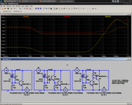
Here it is.
Performance actually decreases, because the Gm of the master transistor is added to that of the slave.
However less drive is required, meaning less requirement placed on the cap. I will simulate next with a 22nH, 70mR cap (realistically ESR for a high voltage cap like this will be much higher, but this is worst case).
- keantoken
Attachments
- Home
- Amplifiers
- Solid State
- Goldmund Mods, Improvements, Stability