Calling Krisfr
Nico,
Now if we can get Krisfr to redraw the schematic............I always like the idea of minimizing the number of junctions in the signal path. If this is agreed upon, now is just a matter of finalizing the details we should be ready for PCB artwork pretty soon, I am assuming that everyone is happy with the front end, I am.
Jam
Last edited:
I will be more than happy to update the schematic. Can we run a simulation?
IF I can get all the right parts in the Schematic, I "THINK" KiCad will run LTSpice. NOT sure but I will give it all a try.
We are making some real progress folks, and that is GREAT...
IF I can get all the right parts in the Schematic, I "THINK" KiCad will run LTSpice. NOT sure but I will give it all a try.
We are making some real progress folks, and that is GREAT...
Krisfr,
..........I think we hit a home run with this design, now to attack the small details.
Jam
..........I think we hit a home run with this design, now to attack the small details.
Jam
Last edited:
Kris, that schematic is very unfinished. Where do Q8 and Q9 connect to the input LTP?
Q1, Q2, Q36, Q37, and Q38 are all wrong. C4 and C34 should be across the diodes, not the resistor, and D17 and D3 should be zeners. Shouldn't input ground go to the top of D7/D8, not the bottom?
Attached is how the shunt reg should look, pay attention! *cracks whip*
- keantoken
Kean:
Please Flesh out these regulators, I am not sure of how the both should be laid out.
I need a little hand holding on this, never seen this configuration and therefore am a little uneasy.
Give me the values of all parts you say are not right...and anybody else got some values, lay um on me. I am here for the next 4-5 hours and I want to put this to bed tonight. I aint Russian but YOU know what I mean...
Thanks...
Last edited:
Shucks I am going senile posted some stuff on Nagys thread. Hope they don't get too wise over there. I wanted to show my board layout for both amp and PSU
Attachments


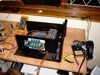

For a moment I was as confused as everyone else on the thread, I think I just created even more confusion posting my boards - hope they don't want to arrange a group buy!
Sorry guys it is 2:30 a.m. and other guys of my age has been snoring for hours. I catch you guys in the moring.
Kindest regards to you all
Nico
Kindest regards to you all
Nico

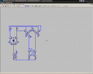
I just got KICAD (learning it), What have we decided on a final circuit ... one like this ?? (below).
I am all for the drivers on the main HS. a small heatsink for the VAS (all 7 devices thermally coupled ). any other ideas.... I am about to create a 6" X 4" (150 X 100mm) draft.
If my friend keen could kindly show me how to add these dang laterals to my library I would also tweak the below circuit. 🙂 Just want to be helpful!!
OS
Attachments

Shucks I am going senile posted some stuff on Nagys thread. Hope they don't get too wise over there. I wanted to show my board layout for both amp and PSU
Absolutely stunning , Nico. That is like my PB250 BJT type layout .. it works well and is easy to implement. 😱😱
OS
OS,
We need to solve the driver or no driver issue, could someone simulate the differences?
Jam
We need to solve the driver or no driver issue, could someone simulate the differences?
Jam
OS,
We need to solve the driver or no driver issue, could someone simulate the differences?
Jam
With or without , no difference to speak of ..THD/FFT. In the real world , the laterals gate capacitances would interact with the Cob of the VAS devices. This is where you would actually have to build it to find out. I have seen this with my first amp kit in the 90's .. it worked and sounded good but the VAS was VERY HOT (20+ ma).
Final design notes
Here are my final comments regarding the amplifier, and no I don't think we are cloning ELD, I think we are developing an amplifier that uses the best of the two designs in order to achieve a performance that will be better than each on their own.
Front End.
Although you have made the right decision on the front end I would like to throw in another two pennies worth.
I have a feeling that using the DC coupling and FETs stands Goldmund in good stead regarding to sound. If one considers that there is no phase change in the bass region (unlike capacitor coupling of input and NFB) may just be why their amp sounds good. At low frequencies our phase perception is much more acute than at higher frequencies.
VAS
The ELD driver using medium power transistors and double Wilson performs better than small signal transistors followed by a driver. It is more linear, easier to compensate.
Output
I would insist that those wanting the most out of the amp uses four pairs of devices with source resistors. Those wanting 100-120 watt can omit two pairs.
Power supply Front end
I have done some listening on my class A headphone amp and HD800 cans, using both a shunt and a series regulator. The shunt regulator sounds healthier, don't ask what that means, it just does.
The front end should be run at 10 -15 V higher than the output stage. For this we need a small transformer of 0-9, 0-9 V (two secondaries) and about 10 VA or so feeding a full wave bridge and followed by at least 1000 uF series resistor (filtering) and another 1000uF cap rated at the operating voltage you choose, followed by the shunt regulator.
The secondaries of the small transformer would be connected in series with the secondaries of the main transformer, thus would always be be 9VAC higher, no matter what main transformer size you choose.
Main power supply
We know that lateral mosfets will only swing around 10V from rails, unlike BJTs therefor the need to run the driver stage at 10 or so voltage higher so that we can get close to rail swing on the outputs.
This has the advantage that we do not have to use an 80V supply to the output devices and it can be dropped to a more manageable and available 65V rails (or lower if you like) The transformer will be more cost effective and if you choose correctly 63V capacitors will do.
Interestingly enough and you can go try it practically, the reservoir caps used for the output stage does not have to be mega farad, you need enough energy to cater for the loudest and lowest signal, hence a 4700 uF capacitor sounded nicer and more fluid than the 40 800 uF that I was using.
I hate hacking equipment that I am using, but I did it for the sake of offering advice. The front end is regulated and that is where it matters most. The amp also sounds more dynamic. Much better than using a regulator on the whole amp as I have been doing.
I hate adjectives but unfortunately thats how we communicate. Therefore dump my use of a regulated amp, it is a waste of money.
I would further use two toroidal transformers with a single secondary for each amp. and mount them on top of each other. Feed the primaries anti phase so that any stray magnetic fields cancel. I do this always else you will have problems with these large transformers near the circuitry.
I have never done this, but it may be possible to fit the transformers into a cut-off coffee tin and pot them which will reduce mechanical vibration and the mount them onto the chassis using a rubber insulator or something similar to decouple them from the rest of the amp, maybe even another box.
More final notes.
Do not compensate the amp using the simulated values, this has to be done once you built it practically. The PCB and all other stray elements will only become apparent practically.
Don't believe the THD figures from the simulations, simulators assumes perfect conditions. If we get two orders of magnitude worse in practice we are still doing damn good at any-ones standards.
Following the power supply guidline, it would apear that the final result will be more cost effective and better suited to our objective that I anticipated with regulation.
Kind regards
Nico
OS, paste these models directly to the schematic.
Then ctrl-right-click on the FET symbols, and follow the attached image as a model. Instance name doesn't matter. You can perform this operation on just one symbol and copy/paste it multiple times.
- keantoken
.SUBCKT MSK1058 1 2 3
* TERMINALS: 1 2 3
M1 9 7 8 8 DMOS L=1U W=1U
RD 1 9 80.4M
RS 3 8 5.28M
RG 2 7 21.4
CGS 7 8 410P
EGD 12 0 7 9 1
VFB 14 0 0
FFB 9 7 VFB 1
CGD 13 14 128P
R1 13 0 1
D1 12 13 DLIM
DDG 15 14 DCGD
R2 12 15 1
D2 15 0 DLIM
DSD 8 1 DSUB
LS 30 3 7.5N
LD 1 9 4N
.MODEL DMOS NMOS (LEVEL=3 THETA=85M VMAX=163K ETA=2.2M VTO=.2 KP=.999)
.MODEL DCGD D (CJO=128P VJ=.6 M=.68)
.MODEL DSUB D (IS=29N N=1.5 RS=61.4M BV=160 CJO=802P VJ=.8 M=.42 TT=252N)
.MODEL DLIM D (IS=100U)
.ENDS
.SUBCKT MSJ162 1 2 3
* TERMINALS: 1 2 3
M1 9 7 8 8 DMOS L=1U W=1U
RD 9 1 110.4M
RS 8 3 25.28M
RG 7 2 17.4
CGS 7 8 760P
EGD 12 0 1 2 1
VFB 14 0 0
FFB 9 7 VFB 1
CGD 13 14 467P
R1 13 0 1
D1 12 13 DLIM
DDG 15 14 DCGD
R2 12 15 1
D2 15 0 DLIM
DSD 9 8 DSUB
LS 8 3 7.5N
LD 1 9 4N
.MODEL DMOS PMOS (LEVEL=3 THETA=90M VMAX=183K ETA=6.5M VTO=-.2 KP=1.109)
.MODEL DCGD D (CJO=467P VJ=.6 M=.68)
.MODEL DSUB D (IS=29N N=1.5 RS=61.4M BV=160 CJO=900P VJ=.8 M=.42 TT=252N)
.MODEL DLIM D (IS=100U)
.ENDS
Then ctrl-right-click on the FET symbols, and follow the attached image as a model. Instance name doesn't matter. You can perform this operation on just one symbol and copy/paste it multiple times.
- keantoken
Attachments

Can you guys give me a list of the part numbers of the devices we've chosen, so I can use them in simulation?
One more thing. What if we flip the VAS buffer upside-down, as per attached schematic? We can use better performing, low-voltage, low-noise NPN's. We could even use the 2N5769. Fed by large resistor means the voltage variation of the VAS and degeneration hardly loads the buffer, who's transconductance is no longer added to that of the VAS. Increasing R5 means better CMRR, if that matters any.
- keantoken
Attachments
Yes you can. In practice I found Q9 causes a lot of trouble. It was originally in ELD if you look at the photo you see a missing transistor.
It simulated perfectly, dropped the distortion by another factor of five, but caused tremendous instability in practice. Don't know why and never cared to find out.
It simulated perfectly, dropped the distortion by another factor of five, but caused tremendous instability in practice. Don't know why and never cared to find out.
- Home
- Amplifiers
- Solid State
- Goldmund Mods, Improvements, Stability