My general rule is 0.5mm for signal, 1.0mm for power, 1 - 2 mm for ground, and 1-5mm for heater (12AX7 at 150mA can be skinny, 2.5A 6080 can't be)....
Digikey has a calculator. PCB Trace Width Calculator
Digikey has a calculator. PCB Trace Width Calculator
I can't imagine tubes sockets on pcb without pcb cuts drilled between any 2 pins except G1, cathodes and fillament where there isn't any issue cathode-fillament isolation ...at least 3mm long.Some cuts may be longer helping with attenuating vibrations as the pcb under the tube can become some sort of a leaf spring with careful design which usually imply pcb cuts between every two pins.
Last edited:
Do you use 1oz or 2 oz copper?
well the price of a 2oz board would probably make you go with 1oz, the price jumps at least 6 times for 2oz. I've been using 4 layer boards at jlcpcb a 4 layer board by default has 1oz outer layers and the two inner layers are .5 oz each, but same price as a two layer board. I use the inner two layers doubled up as either the uninterrupted ground plane or the power plane depending. Its worked out well. Ill even leave the outer layers with most of the non-trace copper still intact then ground that too so basically end up with 2 or 3oz ground plane with 1oz traces. I try to get all traces on the bottom, I only add a top trace when I have to jump a crossing trace sometimes Ill manage only one jump trace on top for the whole layout which makes me happy.
I thought it wasn't cost that much. Wonder 2oz copper would benefit for tube pcb. I think thickness costs more than than copper. I am trying to put all the pcb's that I need into a big one for cheaper then cut out them out. 😀
271mm x 212mm: If i do 1 pcb 1/2 size of this, then it would cost $65 so when I combine both, total is $70.7. So instead of 5 pieces, I would end up 10 pieces for an extra $15 even thought I won't need that many but in case someone wants later.
5 pieces, 1.6 Thickness, 1oz for $29.99
5 pieces, 2.0 Thickness, 1oz for $70.7
5 pieces, 1.6 Thickness, 2oz for $57.7
5 pieces, 2.0 Thickness, 2oz for $95
Last edited:
Great thread -- lots of good tips. I'm following with interest.
I don't mean to throw the thread off the point, but can anyone share a known-good symbol for a standard 9-pin miniature (B9A, etc.) tube socket for Sprint Layout?
I'm just getting started with it, waiting on my first batch of pcbs. I don't know yet if the socket symbol I made will come out right.
Thanks.
Great thread -- lots of good tips. I'm following with interest.
I don't mean to throw the thread off the point, but can anyone share a known-good symbol for a standard 9-pin miniature (B9A, etc.) tube socket for Sprint Layout?
I'm just getting started with it, waiting on my first batch of pcbs. I don't know yet if the socket symbol I made will come out right.
Thanks.
I love Sprint Layout I made several tube socket footprints. When I'm back on my computer tomorrow I can upload them.
Great thread -- lots of good tips. I'm following with interest.
I don't mean to throw the thread off the point, but can anyone share a known-good symbol for a standard 9-pin miniature (B9A, etc.) tube socket for Sprint Layout?
I'm just getting started with it, waiting on my first batch of pcbs. I don't know yet if the socket symbol I made will come out right.
Thanks.
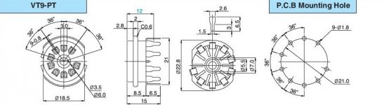
Theres no such thing as standard, Belton allone makes three variants, and the chinese make three noval 9 pin variants that i know of. Then there is CMC which makes one and a couple of others.
Belton VT9PT? is the nicest 9 pin noval around, CMC is just too tight on the tube pins and prohibitively expensive. These are good quality, but three times the price of the Chinese ones.
If you want easy, look up the belton collars for tube shields, and add two holes in the footprint for a m3 spacer that indexes with the tube shield collar. I dont know how sprint works exactly but its best to draw a circle around the spacers akin to the "Keepout" or "Restrict" layer in Eagle so it doesnt short anything to the top plate.
A 3.2mm hole in the center of every tube footprint is a good idea, i like the idea previously mentioned of slotting between G1
Heater routing
i never route heaters on a pcb unless i know the board is going to be fed with DC, for that reason i've inlcuded solder pads for the heater wire connections in some of my footprints. Best to solder those on manually on the same side as the ground plane.
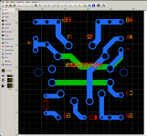
TopoR
There is a Russian autorouter by the name of TopoR, that can eat some of the most common board file formats, and autoroute the board with those very nice looking curved traces. See attached for an example, it eats EAGLE and a couple of other EDA files as input, and you can export back again when you are done. The major benefit of this, is that this autorouter will bend over backwards to accommodate a solution that fits the clearance requirements. and you can be very specific, and specify any clearance between any pair or group of nets manually, this is tedious, but a tube amp board does not require a uniform 0.1'' clearance.
What side should i put the ground plane?
The simplest answer is : on the same side as any snap-in capacitor, and ALLWAYS run the trace for the positive connection on the other side, lest it short to the can of the capacitor.
Attachments
Last edited:
Remember the solder mask is not there to insulate anything, its only job is just to stop solder and provide a surface for printing.
It acts as IR-emissive surface to allow radiative heating in a reflow soldering production line (essential for modern PCB production), it acts as a protective coating against tarnish/oxidation, it helps prevent corona discharge, reduces the chance of short circuit when metal debris is present (yes its a good dielectric)...
Lots of uses/benefits for solder-mask. However its not really good enough for high voltages (say 500V+), and special conformal coatings are probably wise for very high voltage use.
You can silk-screen print directly on uncoated PCB BTW, no special surface is needed for silk-screen inks (just avoid really unwettable materials like PE, PTFE, etc).
Theres no such thing as standard, Belton allone makes three variants, and the chinese make three noval 9 pin variants that i know of. Then there is CMC which makes one and a couple of others.
You may be reading my mind.
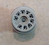
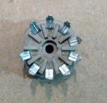
I have a symbol for CMC 9pin socket, but I agree that those are hideously expensive. I bought some sockets that are supposed to be Belton micalex but I don't know exactly which version. The diameter of the circle described by the pins is about 21mm. I've attached photos.
Thanks for the diagrams. Very useful.
Attachments
I love Sprint Layout I made several tube socket footprints. When I'm back on my computer tomorrow I can upload them.
Great thread -- lots of good tips. I'm following with interest.
I don't mean to throw the thread off the point, but can anyone share a known-good symbol for a standard 9-pin miniature (B9A, etc.) tube socket for Sprint Layout?
I'm just getting started with it, waiting on my first batch of pcbs. I don't know yet if the socket symbol I made will come out right.
Thanks.
rongon,
I PM'ed you here with a google share link to go download those Sprint Layout tube socket footprints. If you have trouble getting to the share, I can just email them to you.
Rick
FWIW, All of the sockets I've used on PCB were already in the EasyEDA library... I used the wrong one once and had to buy different sockets lol
kodabmx
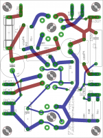
What do you call the two circle holes near 3k3? I like to put some on the traces but couldn't find the term for it. It's better than using 2 square connectors with jumper.
What do you call the two circle holes near 3k3? I like to put some on the traces but couldn't find the term for it. It's better than using 2 square connectors with jumper.
The two "circle holes" are footprints for this vertical resistor.
VERTICAL RESISTOR Resources -
EasyEDA
VERTICAL RESISTOR Resources -
EasyEDA
Well; I am against tube sockets soldered directly to PCBs, but this time I may need to make small boards to mount Compactron sockets... Who has them for Sprint?
Never mind...
Attachments
The two "circle holes" are footprints for this vertical resistor.
VERTICAL RESISTOR Resources -
EasyEDA
Perfect That's what I have been looking for. I searched online but they gave me another one has only 1 end. 🙂
You may be reading my mind.
I have a symbol for CMC 9pin socket, but I agree that those are hideously expensive. I bought some sockets that are supposed to be Belton micalex but I don't know exactly which version. The diameter of the circle described by the pins is about 21mm. I've attached photos.
Thanks for the diagrams. Very useful.
Those are VT9PT from the diagram i posted earlier, best sockets for the job i think. Hole diameter is 1.2mm i think.
Perfect That's what I have been looking for. I searched online but they gave me another one has only 1 end. 🙂
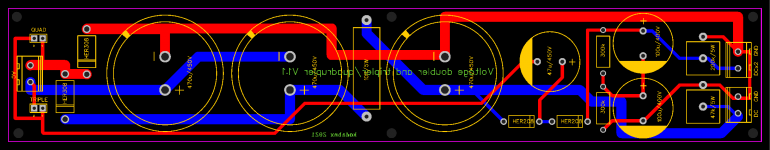
I re-read the thread. Here is an example of a PSU board. Input 120VAC, output 320V/640V however, DCx2 is ~700V unloaded.
I have many of these in service. I've never had any board I've designed arc.
Side note - the jumper for triple doesn't work.
Koda
Attachments
Last edited:
Thanks, I have similar one with 4-470uf caps with choke and bias. That looks neat. Mine is kinda bigger since I have options for tube & diode rectifier. Sometimes, I think point to point PS is more easy to mod later.
- Home
- Amplifiers
- Tubes / Valves
- General rules for designing PCB for valve amplifiers