I'm not clever enough for this. I think I'll have to live without CM's. I've simulated the "Diamante" but never got any good results, probably because of my lack of knowledge.jcarr said:Nelson, Mihai is right. The design of the upper current mirror in your schematic <http://www.diyaudio.com/forums/attachment.php?s=&postid=1739711&stamp=1234201872> is problematic. You may want to redesign this current mirror so that it has double outputs and a single input, feed the input with a current source of the desired value, and feed each of the folded cascodes with one of the current mirror outputs.
Thank you for your suggestions. I didn't know that. I'll move that capacitor.
Also, the present location of C7 may be a problem in real life, because it will allow RF energy injected from the output to short-cut directly to the input stage, without going through any low-pass filter. Better to insert C7 between the gate of J2 and the collector-collector junction of T6/T4 (so it forms a local NFB loop). A revision to the value of C10 may be appropriate if you do this.
regards and hth, jonathan carr
nelsonvandal said:
I'm not clever enough for this. I think I'll have to live without CM's.
Attachments

I'm not clever enough for this.
Don't get discouraged so easily, my good fellow! Please find attached a conceptual schematic.
I think I'll have to live without CM's.
?? You already have been using a CM in your schematics, to sum the differential signals into a push-pull signal that drives the output stage. T1 through T4, then RH and RI will be extremely disappointed to find out that you don't recognize them (^o^)!
I'll move that capacitor.
The original location could have something to do with your impressions of a somewhat piercing sound.
Attachments
jcarr said:The original location could have something to do with your impressions of a somewhat piercing sound.
That and I think CMs should be compensated to overcome overshot in pulse analysis specially complex ones...easily seen in sim, but real circuit probably wouldn't need as much compensation as in sim.
I've been searching high and low to find out a few things about the circuit, I even read the previous jcarr's posts about it but I still don't understand it. Can someone please help clear up a few questions I have with the circuit? 🙁
I'm trying to learn to calculate the DC bias for the circuit (not using simulations)
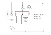
The circuit below does not use any current mirrors but a pair of resistors instead on the drains of the input FETs.
1) How do you define how many currents are running through the folded cascode transistors?
2) What is the relationship between the folded cascode currents and the LED voltage that bias it?
3) How much voltage drop do I need for the LED? Should I use any arbitrary voltage as long as it's enough to forward bias the folded cascode transistors?
4) Long tail pair current = Folded cascode transistor current + Input Pair Current
But because the resistor paired is shared between the drains of the input FETs and the Emitters of the Folded Cascode PNPs I just got lost there O_O!
I'm trying to learn to calculate the DC bias for the circuit (not using simulations)
The circuit below does not use any current mirrors but a pair of resistors instead on the drains of the input FETs.
1) How do you define how many currents are running through the folded cascode transistors?
2) What is the relationship between the folded cascode currents and the LED voltage that bias it?
3) How much voltage drop do I need for the LED? Should I use any arbitrary voltage as long as it's enough to forward bias the folded cascode transistors?
4) Long tail pair current = Folded cascode transistor current + Input Pair Current
But because the resistor paired is shared between the drains of the input FETs and the Emitters of the Folded Cascode PNPs I just got lost there O_O!
thanks for the diagram.
However, I've already calculated those before. It still does not tell me what I should do with the voltage reference nor it clearly defines the current running through the cascode. Sorry if I'm not smart enough to understand this. I'm still quite confused.
Is the Voltage reference picked last when you've decided what currents to run through the folded cascodes and the LTP? It does seem to be pretty "risky" doing that as it'll be quite dependent on the parameters of the transistors.
In my sims, increasing the voltage reference increases the current through the cascodes. This is quite logical as the increase in VBE increases the V drop across the resistors. Do I need higher currents in the f.cascodes in order for them to sound good?
EDIT: OH WAIT, I almost got it.
Given a basic Folded cascode circuit, with current sharing resistors.
LTP CCS = 4mA
Voltage Reference = 2.5V (LM336-2.5)
VBE Drop of BJT transistor = 0.65V
Current Sharing Resistors = 300 Ohms
The current running through the Folded cascode will be:
2.5V - 0.65V = 1.85V
1.85V / 300 Ohms = 6.2mA
Since LTP ccs pulls constant current,
the running current through the folded cascodes is given by
6.2mA - 4mA = 2.2mA.
Am i right?
This kinda works for higher voltage references in my Sims, however if i used TWO 1N4148 diodes with about 0.65V drop on each diode (given around 1.3V total of voltage reference) the current running through the cascodes seems to be VERY VERY low. (this is odd and is contradicting my above calculations).
TzeYang said:thanks for the diagram.
In my sims, increasing the voltage reference increases the current through the cascodes. This is quite logical as the increase in VBE increases the V drop across the resistors. Do I need higher currents in the f.cascodes in order for them to sound good?
This is one of the reasons in using active loading instead of resistors for defining folded cascode current.
jcarr said:
Hint for Mihai's power amp: You can add a DC null control to such a current mirror configuration, which will enable the DC null to function (allowing the entire amp circuit to be direct-coupled) with a minimum of effect on the AC signal, with improvements to the sound quality.
regards and hth, jonathan carr
Thank you for the hint, Jonathan.
I am carefully enough in matching devices, almost like an obsession, hence DC offset is always under 1mV.
Cheers,
Mihai
roender said:
This is one of the reasons in using active loading instead of resistors for defining folded cascode current.
yeah but active loading adds more parts. Some even reportedly said the mirrors sounds yucky. Especially after reading posts from Aksa and so on.
Is my calculations correct on my previous post?
TzeYang said:
yeah but active loading adds more parts. Some even reportedly said the mirrors sounds yucky. Especially after reading posts from Aksa and so on.
Who mention to use mirror?
http://www.diyaudio.com/forums/showthread.php?s=&threadid=111756
Hmmm, you're right.
But the way I look at it, your scheme looks like a "double current mirror". Does not seem any much difference than a current mirror to me. Why does something that is quite similar sound so different instead?
But the way I look at it, your scheme looks like a "double current mirror". Does not seem any much difference than a current mirror to me. Why does something that is quite similar sound so different instead?
Mihai: When you speak of DC offset under 1mV for the RMI-FC100, is this with C21 installed or removed?
If you can consistently get under 10mV without C21 (considering that the RMI-FC100 will not be followed by any subsequent gain stages), I agree that you don't need any DC null adjusters.
regards, jonathan
If you can consistently get under 10mV without C21 (considering that the RMI-FC100 will not be followed by any subsequent gain stages), I agree that you don't need any DC null adjusters.
regards, jonathan
jcarr,
being the guru of folded cascodes, do you find my calculations on the previous page correct?
Thank you.
being the guru of folded cascodes, do you find my calculations on the previous page correct?
Thank you.
Here's how I did one of my foldes cascode designs.
The empty bases/gates have separate PS voltages.
Sigurd
The empty bases/gates have separate PS voltages.
Sigurd
jcarr said:
?? You already have been using a CM in your schematics, to sum the differential signals into a push-pull signal that drives the output stage. T1 through T4, then RH and RI will be extremely disappointed to find out that you don't recognize them (^o^)!
The original location could have something to do with your impressions of a somewhat piercing sound.
Attachments
TzeYang said:being the guru of folded cascodes, do you find my calculations on the previous page correct?
Please, oh cheeky one! I'm allergic to gurus (^o^).
Regarding your post #145:
The circuit below does not use any current mirrors but a pair of resistors instead on the drains of the input FETs.
Not how I would do things, but OK.
1) How do you define how many currents are running through the folded cascode transistors?
The current running through the JFET drain resistors is calculated in the same way as any other base-biased transistor current source. The voltage imprinted across the drain resistors is voltage reference at transistor base minus one Vbe. Once you know the voltage across the drain resistors, derive the current from Ohm's Law.
2) What is the relationship between the folded cascode currents and the LED voltage that bias it?
See above.
3) How much voltage drop do I need for the LED? Should I use any arbitrary voltage as long as it's enough to forward bias the folded cascode transistors?
With resistors as the current sources, the Vref value needs to be whatever gives the target current for the LTP plus folded cascodes. If you want to alter the Vref value without also altering the operating currents, you need to simultaneously juggle the drain resistor values. FWIW, the choice of biasing voltage is much more flexible with active current sources.
4) Long tail pair current = Folded cascode transistor current + Input Pair Current
Input LTP current + folded cascode transistor currents = drain resistor currents.
But because the resistor paired is shared between the drains of the input FETs and the Emitters of the Folded Cascode PNPs I just got lost there O_O!
The drain resistor current is the total current supplied. The LTP grabs whatever current is dictated by the CCS at the JFET sources, and the folded cascodes get whatever is left. The amount of current that the gain circuit uses is therefore always constant (exactly like a super-shunt voltage regulator). In practice, running equal currents through each input JFET and folded cascodes current tends to be a good place to start. So if we say that each of these elements gets one I, the total drain current should be 4I, and each drain resistor should supply 2I.
Any need to similarly go over your post #147?
rgds, jc
Thank you for your kind replies.
I'm aware that I already use a CM, but a CM in that position seems inevitable.
You have given me some work to dig in to, and I don't think simualtions or measurments will do any good, because all active current sources simulate exactly the same. I have to trust my ears.
Even if I use perfect virtual current and voltage sources, I get exactly the same result as when I use the-not-so-good CM, as you can see in the picture below. The pulse response is also exactly the same.
I don't think I can blame the location of the feedback capacitor for the piercing sound. I use it the same way in my other amps (two of them are exactly the same but without CM), and they sound smoother and darker, but from now on I'm going to use the capacitor as per your suggestion. It makes sense.
More suggestions, not only regarding CM, are welcome. Sigurd uses a resistor/capacitor between the collectors of T3/T5 and Mihai is using a transistor in that postition. What's the theory behind this?
Attachments

It's funny how different this amp behaves from "AD797". Adding active current sources to the '797 makes no difference at all in LTSpice.
nelsonvandal said:The pulse response is also exactly the same.
Try this for signal source and let us know what you see when you zoom in at the top/bottom of the leading edge PULSE(-1 1 0 1u 1u 500u 1m). If amplifier clips because of to high voltage, reduce first two ones to something like -.75 .75
nelsonvandal said:Sigurd uses a resistor/capacitor between the collectors of T3/T5 and Mihai is using a transistor in that postition. What's the theory behind this?
If you measure voltage over FC transistors in your circuit, you will see very big difference, dissipation on the left FC Tr is higher than in the right FC Tr. That is because in Michael circuit PNP transistor is put in current mirror input with its base tied to gnd in an attempt to equalised voltage over both FC Trs.
nelsonvandal said:More suggestions, not only regarding CM, are welcome.
For really low distortion you have to put triple emitter follower after VAS (as I have), simple diamond buffer won't do. That way you are reducing loading on VAS and gain output stage current capability by an order of magnitude.😉
jcarr said:
snip
thanks!!!! So it means my calculations were right afterall for the LM326-2.5 situation.
Well, I realized why the 2x1N4148 diodes did not behave well. I looked at the circuit again last night and I realized i did something stupid. The LTP CCS was configured to draw 4mA and it was clearly starving the bias current and leave nothing for the FCascodes. Hike up the voltage reference and i have enough vdrop to generate enough current left for the cascodes ^^
Thanks.
- Status
- Not open for further replies.
- Home
- Amplifiers
- Headphone Systems
- Folded cascode headphone amp