Hello Patrick and fran,
I built one board but ran into issue. I had the one of the current mirror pfet orientation incorrect (Q5a/b). When testing this, the output buffer transistors got really hot. Voltage on output was -11V.
Once I corrected the direction of pfet, I quickly checked by turning on the circuit for few seconds and I still see -10V on the output. I am scared to keep the circuit running since it may damage some other component. Any guidance on how to proceed? Is it safe to run the circuit for debugging?
Thanks
Ok, I have found the issue.
Q8 is supposed to be K170 but I see it is J74. Basically, the quad K170 I bought from diyaudio store had sent one of the transistors in Quad K170 as J74. For a moment, I thought I might have soldered from nnpp set but that set still has k170 and j74. So, I will build the other board and check and will contact the store and check about replacement.
Moral - read and confirm the components before soldering.
Thanks
Most likely some other transistors are damaged.
You need to remove them all and test one by one.
Either will a transistor tester, or many information on the internet.
And you should be using lab supplies with current limit set to ~30mA.
Patrick
You need to remove them all and test one by one.
Either will a transistor tester, or many information on the internet.
And you should be using lab supplies with current limit set to ~30mA.
Patrick
Hello Patrick,Most likely some other transistors are damaged.
You need to remove them all and test one by one.
Either will a transistor tester, or many information on the internet.
And you should be using lab supplies with current limit set to ~30mA.
Patrick
It is almost impossible to desolder the components correctly. I will try first with replacement k170. It will take lot of time to procure. If it does not work, then not sure what to do. For now, let me build the second board and check.
Thanks
Hello Patrick
I replaced the pfet J74 that was accidentally soldered at Q8 with nfet J170 and I got the output offset to 50mV. Later, I realized that both jfet's in output stage needs to be matched and hence I changed the other nfet (Q7) as well from the matched pair of nfet's. After this change, I get offset close to 2mV. So I think the board is working fine now. I will keep the power supply on for some time and check if offset drifts.
On the other board, the first power up yielded output offset of around 2.5mV and I assume is fine as well.
Once I check the output offset 10-15mins after applying power supply and making sure it is fine, I will connect it to DAC and check. Thanks to you and Fran for this circuit, group buy and support.
Thanks
Balaji

In case someone has matched zvp4424 and zvn3306 please let me know.
That would save me from matching them myself (though it is a good practical skill to learn 🙂 )
That would save me from matching them myself (though it is a good practical skill to learn 🙂 )
it is a good practical skill to learn
I can only encourage that you get 25+ of each.
Match them for your own use.
And share any remaining matched sets with other builders.
Patrick
Hello Patrick,
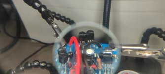
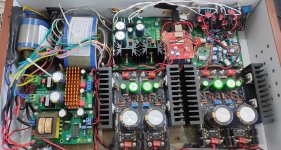
I wanted to document my FC CEN IV build here so that it will be helpful for others. I built my boards for AD1862 DAC and had multiple churns to get it working.
1. After initial build and getting the output bias close to 0mV, I tried playing from the DAC but there was no sound. I was wondering if the DAC board had an issue but the DAC worked earlier with opamp output stage. So, I started debugging the IV boards.
2. As part of debugging, I found out that Rt3 and Rt4 should be present else the circuit will not work. I was thinking these resistors are needed for adjusting bias through MOSFET and since I got matched MOSFET's and resistors from Fran, I thought I can skip Rt3/Rt4. Once I realized they are needed, I soldered them on and then I noticed offset moving lot more than before. I feel this is a good way to build this circuit. First build the boards without Rt3/Rt4 and ensure the offset is low (you will ensure other part of circuit is fine and not risk the MOSFET's). Then you can add Rt3/4 and continue. Let me know what you think about this.
3. Once I was done with this, I did not thermally couple the current mirrors and input/output pairs. This caused the offset to wander a lot more than I expected. Once I thermally coupled them with slight dab of heatsink paste and heat shrink wrap, it became more stable. So it is important not to skip this step.
4. Once I had offset close to 10mV, I tried playing through it and I noticed that the offset is stable without any inputs but when I connected it to laptop through the USB board, it starts wandering. I later realized may be this is normal since this is IV converter and this is expected? Please let me know if my understanding is correct.
5. After all this, I connected it to test speakers and heard music. I was very happy to have completed this build. I will let it settle for sometime before I check it in my main system.
Please let me know your thoughts on some of the above points.
Thanks
Balaji
Attachments
@baswamin - its always good to post your experience and it helps others.
As regards R3t/R4t - yes, you need those - the default value in the BoM is given as 20r, but they can be used to adjust drain voltage of Q1/Q2:
Thermal coupling is important for stability for sure...
As regards the offset wandering around when it is connected to the USB etc - I don't know what that is.... is there a chance there is signal coming from the laptop through the DAC and confusing your meter? I'm taking it that the offset you are seeing here is low? Could it be that you have some low amplitude high frequency noise coming through that your meter is interpreting as DC? I think this is something that is hard to figure out remotely, but it is clear it is coming from before the FC CEN as you mention it is stable on its own.
Enjoy the listening!
As regards R3t/R4t - yes, you need those - the default value in the BoM is given as 20r, but they can be used to adjust drain voltage of Q1/Q2:
Rt3,4 allow you to fine trim the drain voltage of Q1,2 to 7.5V for optimal operating point.
If you don't want to trim, use anything between 0 to 30R at both positions.
Thermal coupling is important for stability for sure...
As regards the offset wandering around when it is connected to the USB etc - I don't know what that is.... is there a chance there is signal coming from the laptop through the DAC and confusing your meter? I'm taking it that the offset you are seeing here is low? Could it be that you have some low amplitude high frequency noise coming through that your meter is interpreting as DC? I think this is something that is hard to figure out remotely, but it is clear it is coming from before the FC CEN as you mention it is stable on its own.
Enjoy the listening!
When I built my FC CEN the cascode mosfets were difficult to source, and eBay was where I ultimately purchased them. Good news is that DigiKey now shows plenty of stock for both.
It is good to know that there are still fans after 2.5 years.
And for those interested in a less costly solution, if you believe in distortion measurements, passive IV with a 27R resistor + a 100x gain stage with AD797 has almost the same signature.
www.diyaudio.com/community/threads/distortion-measurements-of-a-collection-of-iv-converters.415094/
Worth a try.
www.diyaudio.com/community/threads/dac-ad1862-almost-tht-i2s-input-nos-r-2r.354078/post-7319854
www.diyaudio.com/community/threads/dac-ad1862-almost-tht-i2s-input-nos-r-2r.354078/post-7319860
www.diyaudio.com/community/threads/dac-ad1862-almost-tht-i2s-input-nos-r-2r.354078/post-7319888
Patrick
We actually tested a few more in the link above.
But they were someone else's products.
So we do not publish.
Just for own interest.
And Fran agrees with you 100%. 😊
But we have also built the SMMS IV from Sergio.
It has the best distortion numbers, if that is deciding.
Patrick
But they were someone else's products.
So we do not publish.
Just for own interest.
And Fran agrees with you 100%. 😊
But we have also built the SMMS IV from Sergio.
It has the best distortion numbers, if that is deciding.
Patrick
Another option is to do some measurements and try to identify the broken part ...Hello Patrick,
It is almost impossible to desolder the components correctly. I will try first with replacement k170. It will take lot of time to procure. If it does not work, then not sure what to do. For now, let me build the second board and check.
Thanks
Jan
We actually tested a few more in the link above.
But they were someone else's products.
So we do not publish.
Just for own interest.
And Fran agrees with you 100%. 😊
But we have also built the SMMS IV from Sergio.
It has the best distortion numbers, if that is deciding.
Patrick
And how does it compares, please ?
Do you think the less costly AD8597 could gives soundwize as good results ?
That has long been published by Fran in one of his audition reports.Do you think the less costly AD8597 could gives soundwize as good results ?
www.diyaudio.com/community/threads/dac-ad1862-almost-tht-i2s-input-nos-r-2r.354078/post-7264825
Patrick
If that's what pleases you, it is all that matters.I was blown away by the 5534 when I first fired up my Miro AD1862 dac.
Audio is all subjective in the end.
😊
Patrick
- Home
- Source & Line
- Digital Line Level
- Folded Cascode CEN IV with fixed Rails